
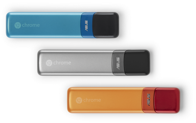
ASUS Launches The Chromebit CS10 HDMI Stick
| ASUS Chromebit CS10 | |
| SoC | Rockchip RK3288-C 4 x Cortex A17 + Mali T764 |
| RAM | 2 GB LPDDR3 |
| NAND | 16GB NAND |
| Dimensions / Mass | 123 x 31 x 17mm, 75g |
| OS | Chrome OS |
| Other Connectivity | 2x2 802.11a/b/g/n/ac + BT 4.0, HDMI 1.4, USB 2.0, DC-in |
| Price | $85 |
A combination of size and price means we're not going to be seeing something like an Intel Core i5 in an HDMI stick any time soon. Thankfully, Chrome OS tends to run pretty well even with minimal hardware power. At $85, the Chromebit CS10 comes with 2GB of RAM, 16GB of eMMC NAND, dual-band 802.11ac, and a Rockchip RK3288-C SoC. RK3288-C is a quad core Cortex A17 part paired with a Mali T764 GPU. The same SoC has actually shown up in some of ASUS's actual Chromebooks as well, so it's not surprising to see it in the Chromebit.
As with all HDMI sticks, you still need a separate power adapter because HDMI 1.4 can't supply nearly enough power for even such a smaller computer. Even with that, the Chromebit could still make for an interesting computer of sorts that can be taken anywhere in your pocket.
The ASUS Chromebit CS10 will cost $85, and it comes with a year of 100GB Google Drive space. It'll begin shipping today.
Read More ...
Best Android Phones: Holiday 2015
We'll be starting things off this year with smartphones. Smartphones are an enormous market, and the average phone lifetime still being only 18-24 months, many gifts given this holiday season are going to be smartphones. So let's take a look at what we believe to be the best Android phones that you can buy this holiday season.
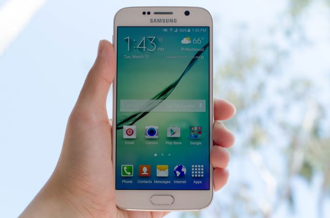
Best Android Phablet: Samsung Galaxy Note5
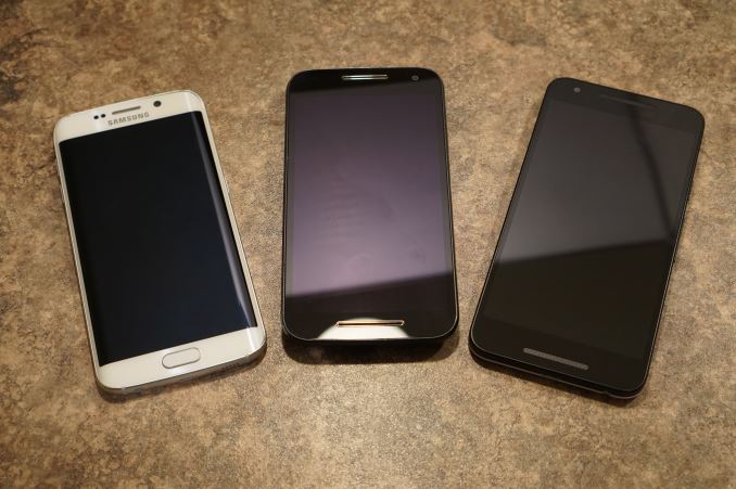
The term phablet is a bit silly in my opinion, but it has become a fairly common term to describe smartphones with very large profiles. The definition of a phablet is not exactly concrete, and it mainly has to do with a device's chassis size. For example, the Nexus 6 and Galaxy Note5 are clearly phablets, and it's fairly safe to say that the iPhone 6s Plus is one too. However, I don't know if I would describe the LG G4 as a phablet. It has the same screen size as the iPhone 6S Plus, but the use of on-screen buttons and smaller overall chassis size mean that it ends up straddling the line between your standard smartphone and a phablet. When looking at which devices are available in many regions, I think it's pretty clear which phablet offers the best value at the absolute high end, and which offers the best value for someone who is looking to spend less than what they would on a typical flagship.
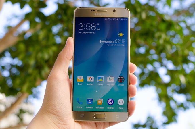
I don't think it would be wrong to say that Samsung really pioneered the phablet category. The original Galaxy Note was laughed at by many, but as time has gone on Samsung has improved on it, and now every vendor offers a similarly sized device. With that in mind, it shouldn't come as a surprise that the Galaxy Note5 is my recommendation for a high end phablet. It comes with everything that makes the Galaxy S6 a great phone, but in a larger size and with some additional improvements. Just as an overview, you're getting a 5.7" 2560x1440 AMOLED display, Samsung's Exynos 7420 SoC, 4GB of LPDDR4 RAM, and 32, 64, or 128GB of internal NAND. Some differences from the Galaxy S6 apart from simply being larger include improved camera image processing, making it a serious contender for the title of best smartphone camera, and the inclusion of Samsung's S-Pen for navigation and drawing.
The Galaxy Note 5 costs $699 for the 32GB version in the US. There are often deals that can help bring the price down a bit, such as a recent $50 off offer from T-Mobile. The 64GB model bumps the price to $779. It's worth noting the prices for the Galaxy S6 Edge+ as well, which is to the Galaxy Note5 what the Galaxy S6 Edge is to the standard Galaxy S6. It starts at $779 for 32GB, and $859 for 64GB. I personally think the edge design looks cool, but there's definitely a trade off in terms of ergonomics, and I don't think it's worth the additional cost unless you really want to own Samsung's absolute highest end phone.
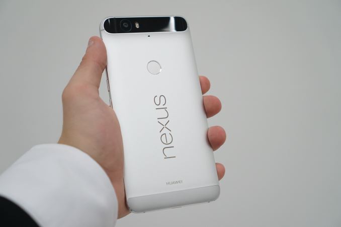
For buyers who aren't fans of the Galaxy Note5, or who are looking for something that isn't quite as expensive, the Nexus 6P is definitely worth considering. Like the Galaxy Note5 it has a 5.7" 2560x1440 AMOLED display, but inside you get Qualcomm's Snapdragon 810 paired with 3GB of LPDDR4 RAM and 32GB of NAND.
Some highlights of the Nexus 6P are the camera and the chassis. While we haven't published our Nexus 6P review yet, it uses the same sensor and lens arrangement as the Nexus 5X which I felt has one of the best cameras of any smartphone. The aluminum chassis of the 6P may also be more appealing than the metal/glass design of the Note5, although I didn't feel that the design and ergonomics were at the same level as devices like Huawei's own Mate S or the iPhone 6s Plus.
Of course, the biggest appeal of the Nexus 6P is its price. At $499 for 32GB, it undercuts most flagship phablets by $200 or so, while being competitive in many other respects. You definitely lose out on the performance of Samsung's Exynos 7420 SoC, but there are obviously tradeoffs that are made when targeting a lower price. The promise of software updates along with a great camera, an aluminum build, and a great fingerprint scanner make the Nexus 6P a very worthwhile choice for a phablet at a lower price than the latest and greatest flagships. European customers will notice that they get charged a significant premium for the Nexus 6P, with the 32GB model priced at around 700€. At that price I would probably consider other devices unless one is determined to stay with a Nexus phone for the support and updates.
Best High-End Android Smartphone: Samsung Galaxy S6
While phablets have grown immensely in popularity, the normal flagship devices from the players in the Android space tend to be smaller than the 5.7-6.0" displays that ship on phablets. Not having to push a large size also opens up more opportunities to offer a great device at a lower price than the competition. Taking that into consideration, I think there are two key flagship devices that are worth considering if looking for a flagship phone in a typical size, along with one clear winner for a smartphone that offers a lot for a lower price than flagship smartphones.
The Galaxy S6 really needs no introduction. Along with the Note5 it's really the only Android phone this year that was able to push the performance of Android devices forward, courtesy of its Exynos 7420 SoC. Along with still being the fastest Android phone around, the Galaxy S6 comes with a top notch 5.1" 2560x1440 AMOLED display, 3GB of LPDDR4 RAM, 32, 64, or 128GB of NAND, and the same 16MP camera that the Galaxy Note5 uses.
It is a bit disappointing that the Galaxy S6 is still the fastest Android phone out there many months after it was released. While some may feel it's actually best to wait for the next generation Galaxy phone from Samsung, such a launch is still one or two quarters away, and if someone is looking to get the most powerful Android smartphone for the holidays the Galaxy S6 is definitely it. As far as the price goes, the fact that the S6 is a bit older now means you can find some appealing discounts. Right now on T-Mobile USA you can get the 32GB model for $579, and at $659 you get 128GB which is a pretty great deal. Like the Note5, I wouldn't recommend paying the extra money for the Edge version of the phone unless you really want the more unique design, as the ergonomics are honestly a downgrade.
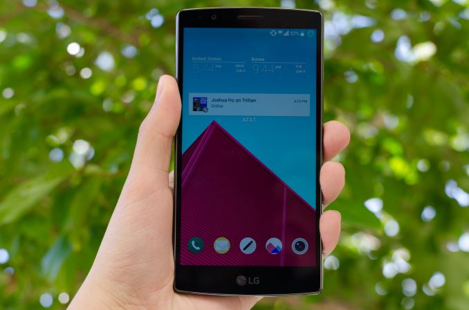
If you're looking for something a bit larger, or less expensive than the Galaxy S6, the LG G4 is definitely worth considering. Although it has a 5.5" display, it's much smaller than a phone like the iPhone 6s Plus due to its small bezels on all sides, and the use of on screen buttons. In my experience it's still a bit too big to be used comfortably in a single hand even with affordances like the back-mounted volume rocker, but it's not really a phablet either. As far as its specs go, you get Qualcomm's Snapdragon 808 SoC, 3GB of LPDDR3 RAM, 32GB of NAND, and a 16MP Sony IMX234 rear-facing camera. It also has microSD expansion and a removable battery for the users who were upset with Samsung's removal of those features on this year's Galaxy flagships.
Price wise, the LG G4 sells for around $479, which is about $100 less than you'd pay for the Galaxy S6. The size of the phone is definitely worth considering in addition to the price, as the S6 is much easier to use with a single hand, but if you want a phone with a larger display without moving completely into phablet territory the G4 is definitely a phone to heavily consider.
Best Mid-Range Android Smartphone: Google Nexus 5X
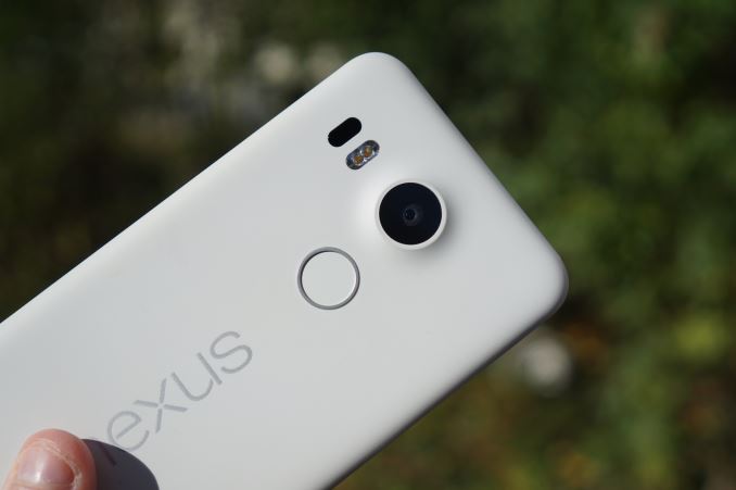
Next we come to the lower cost high end, and here's there's only one real Android device worth mentioning, the Nexus 5X. This is actually my personal favorite Android device from this year, and I published my review of it last week. In many ways it's similar to the LG G4, which isn't surprising when you consider that it's made by LG. It has a Qualcomm Snapdragon 808 SoC, 2GB of LPDDR3 RAM, 16 or 32GB of NAND, and the same great 12MP camera that you get in the Nexus 6P.
To sum up my thoughts on the Nexus 5X from my review, I'll say that it's imperfect, but I think it's unbeatable at $379. Snapdragon 808 doesn't deliver the performance jump that you'd expect from two years of technological advancement since the Nexus 5, but you still get a great display, an amazing camera, good battery life, a quick and simple fingerprint scanner, and a plastic but very solid chassis. The fact that the 5X includes the same camera as the Nexus 6P at its $379 price is really what gives it an edge, and if you're looking to get something smaller than a phablet without paying the $600-700 commanded by flagship phones I don't think you can go wrong with the Nexus 5X. Like the 6P, the 5X is unfortunately more expensive in Europe, coming in at around 449€, and so in those markets it may be best to consider some other options.
Best Budget Android Phone: Motorola Moto G (2015)
The last category on the list is the budget phone, which to me includes anything from $250 down, although $250 is certainly pushing it. There are certainly a large number of Android devices that fit this category, and I'm sure some people will feel that it makes the most sense to look at importing phones from Xiaomi rather than buying a phone from a more global brand where you may not get as much for your money. I can only really speak from experience, and I think importing comes with its own issues regarding the warranty, customs fees, and carrier compatibility. There was only one budget device from the big Android players that I looked at this year and feel is really worth considering, and it's the 2GB version of the 2015 Moto G.
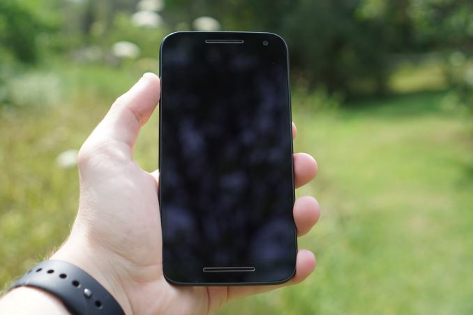
The 2015 Moto G comes in two versions. Both have a Qualcomm Snapdragon 410 SoC, a Sony IMX214 13MP camera, and a 1280x720 IPS display. However, while $179 gets you a version with 8GB of NAND and 1GB of RAM, $219 doubles both of those to 16GB and 2GB respectively. With the amount of RAM overhead created by Java applications that use garbage collection I really don't think 1GB is a usable amount of memory on an Android device unless you're shopping in the sub $100 range where you're not likely to be using many apps at all. For that reason, I think the 2GB model is the best budget smartphone, as it includes a relatively good camera for its price, has enough RAM, and should be fast enough for the needs of anyone shopping for a smartphone at this price. It's also waterproof, and has an extremely long battery life.
While there are other budget Android phones, you end up having to pay significantly more than the Moto G to get any significant improvement, and dropping the price even lower ends up coming with a number of compromises that aren't worth the money you save.
Read More ...
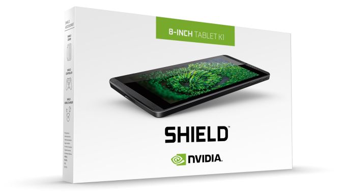
NVIDIA Re-launches the SHIELD Tablet as the SHIELD Tablet K1
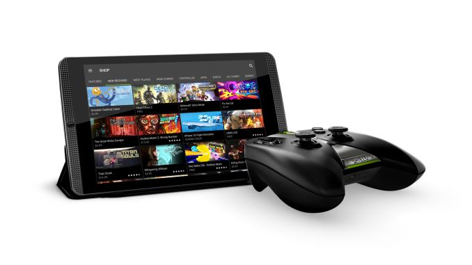
Today NVIDIA is re-introducing the SHIELD Tablet with a new name. It's now called the SHIELD Tablet K1, something I hope implies we will soon see a SHIELD Tablet X1.
While the name is new, we're looking at the exact same tablet that launched last year. I've put the specs in the chart below as a refresher.
| NVIDIA SHIELD Tablet K1 | |
| SoC | NVIDIA Tegra K1 (2.2 GHz 4x Cortex A15r3, Kepler 1 SMX GPU) |
| RAM | 2 GB DDR3L-1866 |
| NAND | 16GB NAND + microSD |
| Display | 8” 1920x1200 IPS LCD |
| Camera | 5MP rear camera, 1.4 µm pixels, 1/4" CMOS size. 5MP FFC |
| Diameter / Mass | 221 x 126 x 9.2mm, 390 grams |
| Battery | 5197 mAh, 3.8V chemistry (19.75 Whr) |
| OS | Android 5.1.1 Lollipop |
| Other Connectivity | 2x2 802.11a/b/g/n + BT 4.0, USB2.0, GPS/GLONASS, Mini-HDMI 1.4a |
| Accessories | SHIELD DirectStylus 2 - $19.99 SHIELD Controller - $59.99 SHIELD Tablet K1 Cover - $39.99 |
| Price | $199 |
The NVIDIA SHIELD Tablet K1 still has NVIDIA's Tegra K1 SoC, with four Cortex A15 cores and the incredibly fast single SMX Kepler GPU. The SoC is paired with 2GB of LPDDR3 RAM and 16GB of NAND, with the original 32GB model being dropped. There's still microSD expansion for storing media, and with Android Marshmallow expandable storage will lose much of its third class status on Android which will be helpful.
Of course, the biggest change here beyond the fact that the SHIELD Tablet is being put back on sale is its new price. At $199 it's $100 cheaper than when it first launched, and it makes it one of the only good tablets that you can actually get at that price point with the Nexus 7 having been gone for some time now. NVIDIA's optional accessories are all available as well, and if you plan to use the gaming features of the SHIELD Tablet K1 I would definitely factor the price of the controller into your cost consideration. In any case, it's good to see the SHIELD Tablet K1 back on sale, and at $199 I think it's definitely worth considering if you're looking for a tablet at that price.
Read More ...
AMD Releases Catalyst 15.11.1 Beta Drivers
Overall this driver is a very straightforward performance driver, with AMD pushing out a batch of performance optimizations for Star Wars: Battlefront, Fallout 4, Assassin's Creed Syndicate, and Call of Duty: Black Ops III. Otherwise there are no bug fixes listed, though AMD does list some known issues, including that Assassin's Creed Syndicate and Star Wars: Battlefront cannot launch in full screen mode on some laptops with an Intel CPU and an AMD GPU.
Meanwhile, it’s worth noting that this is likely one of the last Catalyst driver releases we’ll see from AMD. Earlier this month AMD announced their new Crimson driver branding and overhaul of their control center, and while AMD has not announced a specific launch date yet, we do know it’s expected before the end of the year, only a short 6 weeks away.
Anyhow, as always those interested in reading more or installing the updated beta drivers for AMD's desktop, mobile, and integrated GPUs can find them on AMD's Catalyst beta download page.
Read More ...
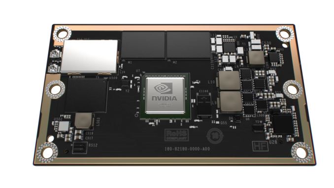
NVIDIA Announces Jetson TX1 - A Tegra X1 Module & Development Kit
However since it was a full COTS implementation of Tegra K1, something unexpected happened for NVIDIA: developers started using Jetson TK1 outright as a production board. For small developers doing similarly small product runs, or just projects that didn’t require a highly integrated solution (e.g. embedded systems as opposed to mobile devices), some developers would just stick with Jetson since it meant they could skip system hardware development and focus on software and/or peripherals.
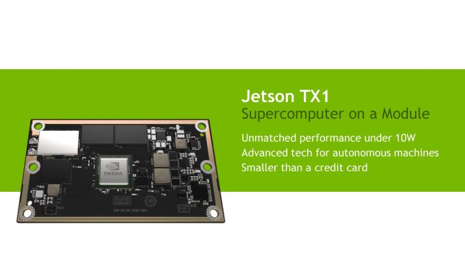
Moving on to the present, after announcing their latest-generation Tegra X1 SoC at CES 2015 and integrating it into some of their own products over the past several months (Drive PX, SHIELD Console, etc) NVIDIA is now rolling out an updated Jetson product based on the X1. The latest Jetson, which NVIDIA is appropriately calling the Jetson TX1, is designed to refresh the platform with the more powerful Tegra X1 SoC and its full ARMv8 AArch64 CPU + Maxwell GPU capabilities. At the same time however, based on their unexpected success as a COTS product, NVIDIA has redesigned Jetson to better serve the COTS market while also continuing to serve the Tegra developer kit market.
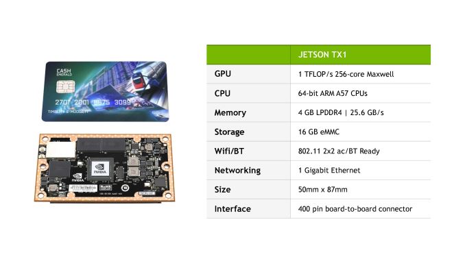
The end result is that for its TX1 iteration Jetson has been split in two, and now comes as stand-alone compute module with a separate carrier board for I/O. The Jetson TX1 module itself – which is for all practical definitions Jetson TX1 in its entirety – contains a full working TX1 system. NVIDIA tells us that Jetson TX1 should offer 2-3 times the performance of Tegra K1, particularly where the GPU is involved, and while we don’t have the CPU clockspeed some quick math on NVIDIA’s 1 TFLOPS claim puts the GPU clockspeed at 975MHz (assuming FP16) with the complete module rated for approximately 10W.
Otherwise along with the TX1 SoC, NVIDIA has attached 4GB of LPDDR4-3200, a 16GB eMMC flash module, a 2x2 802.11ac + Bluetooth wireless radio, and a Gigabit Ethernet controller. By providing a complete TX1 system on a board a bit smaller than a credit card, NVIDIA is looking to further the COTS usage of Jetson by giving product developers a smaller dedicated board specifically designed for COTS usage and quick integration into shipping products.
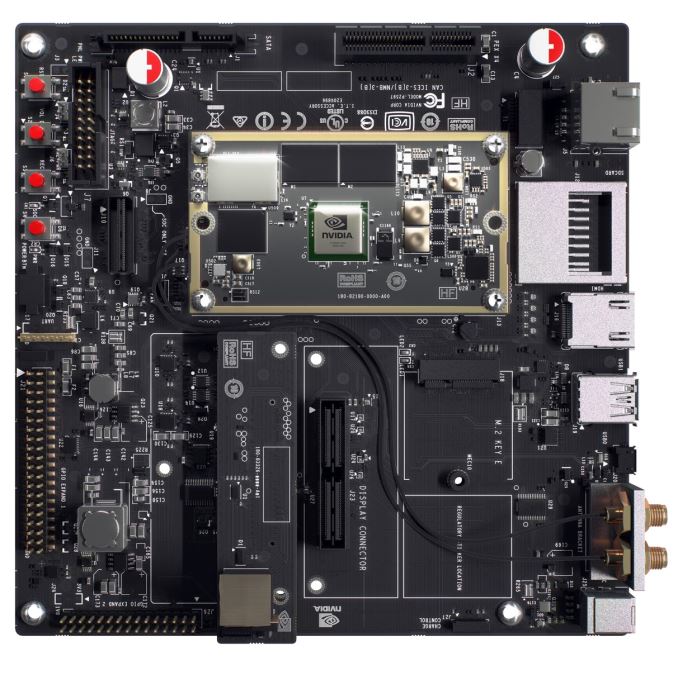
Meanwhile I/O connectivity is now provided by a separate board, be it a product-specific developer design or the official Jetson TX1 carrier board, with the Jetson TX1 using a 400 pin board-to-board connector to attach to other devices. Similar to the original Jetson TK1, the official Jetson TX1 carrier board is designed to offer TX1 as a development kit and contains a full suite of I/O including Ethernet, WiFi + BT antenna connectors, HDMI, USB, M.2, a large number of GPIOs, a camera serial interface with 5MP camera, and a PCIe 2.0 x4 slot. Relative to Jetson TK1, the newer TX1 includes more GPIOs, the camera, a full-size PCIe interface, and it can now work from a more traditional 3.3v power supply.
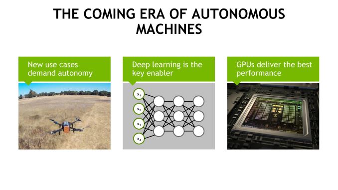
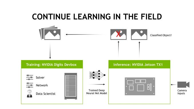
Moving on, not unlike TX1’s discrete GPU counterparts, with the Jetson TX1 platform NVIDIA is strongly focusing on machine learning and autonomous machines. The company believes that machine learning is the next great frontier for GPUs – both discrete and integrated – and is capitalizing on neural net research that has shown GPUs to be capable of both quickly training and quickly executing neural nets. This is an important differentiator for NVIDIA given their strengths in GPU development (both from a tech perspective and overall SoC GPU performance), and because it is a market that they feel no one else is truly aiming for (or at least competitive in) at this time. The Drive PX system already uses TX1 on this basis, and now with Jetson TX1 NVIDIA is looking to extend that relationship to a much wider group of developers.
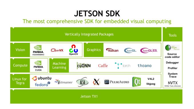
Similar to Jetson TK1 then, Jetson TX1 comes with a suite of software and SDKs in order to simplify the development process and to give developers a good starting point for implementing machine learning. Along with the Linux for Tegra environment, NVIDIA is including their cuDNN neural network library and VisionWorks computer vision toolkit. Coupled with other APIs and software packages such as OpenVX and various neural network systems, NVIDIA is aiming to make the Jetson SDK an ecosystem in and of itself.
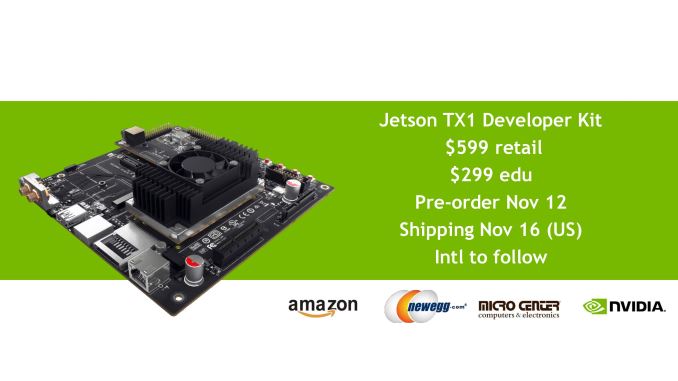
Finally, along with today’s announcement NVIDIA also unveiled the pricing and availability of the Jetson TX1 module and the full development kit. NVIDIA will begin taking pre-orders for the dev kit on the 12th with kits to start shipping as soon as the 16th, and will sell for $599 retail/$299 education. The dev kits will contain the module, carrier board, camera board, a heatsink-fan for cooling (which we’re told is grossly overpowered for TX1), and all of the necessary cables. Meanwhile the stand-alone Jetson TX1 module for use in commercial products will go on sale in Q1 of 2016, priced at $299 in 1K quantities.


Read More ...
Qualcomm Snapdragon 820 Experience: HMP Kryo and Demos

In power, Qualcomm published a slide showing average power consumption using their own internal model for determining days of use. In their testing, it shows that Snapdragon 820 uses 30% less power for the same time of use. Of course, this needs to be taken with appropriate skepticism, but given the use of 14LPP it probably shouldn’t be a surprise that Snapdragon 820 improves significantly over past devices.
The other disclosures of note were primarily centered on the CPU and modem. On the modem side, Qualcomm is claiming 15% improvement in power efficiency which should eliminate any remaining gap between LTE and WiFi battery life.
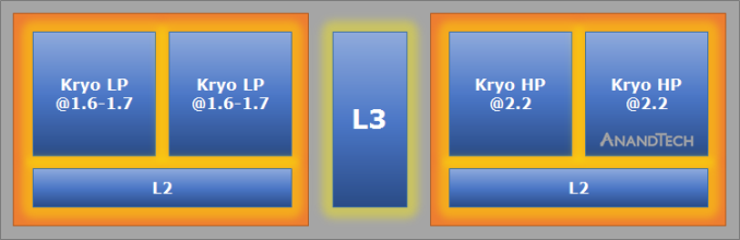
On the CPU side, while the claims of either doubled performance or power efficiency have been discussed before, new details on the CPU include that the quad core CPU is best described as an HMP solution with two high-performance cores clocked at 2.2 GHz and two low-power cores clocked at 1.6 or 1.7GHz when looking at previous Qualcomm SoCs with two clusters that share an architecture. Qualcomm also disclosed that the CPU architectures of both clusters are identical, but with differences in cache configuration. However, the differences in cache configuration weren’t disclosed. I wasn't able to get an answer regarding whether this is an ARM big.LITTLE design that uses CCI-400 or CCI-500, but given that there's an L3 cache shared between clusters it's more likely that this is a completely custom HMP architecture.
In addition to these disclosures, we saw a number of demos. Probably the single most interesting demo shown was Sense ID, in which it was shown that fingerprint sensing worked properly through a sheet of glass and aluminum. To my recollection both the glass and aluminum were 0.4mm thick, so the system seems to be relatively robust. For those unfamiliar with Sense ID, rather than relying of high-resolution capacitive touch sensing the system uses ultrasonic sound waves to map the fingerprint, which allows it to penetrate materials like glass and metal and improves sensitivity despite contaminants like water and dirt.

One area of note was that Qualcomm is now offering their own speaker amp/protection IC that would compete with ICs like the NXP TFA9895 that are quite common in devices today. The WSA8815 chip would also be able to deliver stereo sound effects in devices with stereo front-facing speakers. It seems that the primary advantage of this solution is cost when bundled with the SoC, but it remains to be seen whether OEM adoption would be widespread.
One of the other demos was improved low light video and photos by using the Hexagon 680 DSP and Spectra 14-bit dual ISP. The main area of interest in this demo was improved visibility of underexposed areas by boosting shadow visibility, while also eliminating the resulting noise through temporal noise reduction.
On the RF side, in addition to showing that the Snapdragon 820 modem is capable of UE Category 12/13 LTE speeds Qualcomm also demonstrated that the Snapdragon 820 is capable of dynamically detecting WiFi signal quality based upon throughput and other metrics that affect VOIP quality and seamlessly handing off calls from WiFi to LTE and back. We also saw a demo for Qualcomm’s closed-loop antenna tuning system which allows for reduced impedance mismatch relative to previous open-loop antenna tuners which loaded various antenna profiles based upon things like touch sensing of certain critical areas.
Read More ...
ARM Announces New Cortex-A35 CPU - Ultra-High Efficiency For Wearables & More
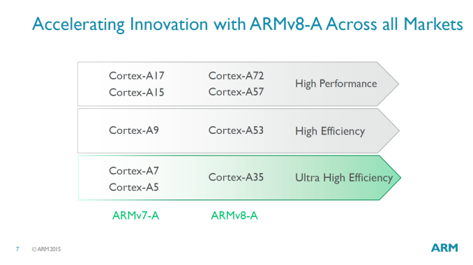
What seems to be counter-intuitive is that ARM sees the A35 not as a successor to the A53, but rather a replacement for the A7 and A5. During our in-depth analysis of the Cortex A53 in our Exynos 5433 review earlier this year I claimed that the A53 seemed to be more like an extension to the perf/W curve of the Cortex A7 instead of it being a part within the same power levels, and now with the A35 ARM seems to have validated this notion.
As such, the A35 is targeted at power targets below ~125mW where the Cortex A7 and A5 are still very commonly used. To give us an idea of what to expect from actual silicon, ARM shared with us a figure of 90mW at 1GHz on a 28nm manufacturing process. Of course the A35 will see a wide range of implementations on different process nodes such as for example 14/16nm or at much higher clock rates above 2GHz, similar to how we've come to see a wide range of process and frequency targets for the A53 today.
Most importantly, the A35 now completes ARM's ARMv8 processor portfolio with designs covering the full range of power and efficiency targets. The A35 can also be used in conjunction with A72/A57/A53 cores in big.LITTLE systems, enabling for some very exotic configurations (A true tri-cluster comes to mind) depending if vendors see justification in implementing such SoCs.
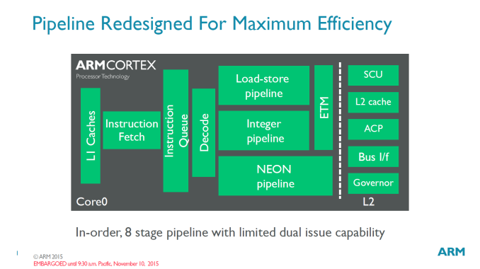
At
heart, the A35 is still an in-order limited dual-issue architecture
much like the A7 or A53. The 8-stage pipeline depth also hasn't changed
so from this high-level perspective we don't see much difference in
comparison to preceding designs. What ARM has done though is to
improve the individual blocks for better performance and efficiency by having bits and pieces of architectural enhancements that are even newer than what big cores such as the A72 currently employ.
Areas
where the A35 had focused attention on are front-end efficiency
improvements, such as a redesigned instruction fetch unit that improves
branch prediction. The instruction fetch bandwidth was balanced for
power efficiency while the instruction queue is now smaller and also
tuned for efficiency.
It's
especially on memory benchmarks where the A35 will shine compared to
the A7: The A35 adopts a lot of the Cortex A53's memory architecture. On
the L1 memory system of which A35 can have configurable 8 to 64KB of
instruction and data caches we now see use of multi-stream automatic
data prefetching and automatic write stream detection. The L2 memory
system (configurable from 128KB to 1MB) has seen increased buffering
capacity and resource sharing while improving write stream efficiency
and introducting coherency optimizations to reduce contention.
The
NEON/FP pipeline has seen the biggest advancements, besides improved
store performance the new units now add fully pipelined double precision
multiply capability. The pipeline has also seen improvements in terms
of area efficiency, part of the reason enabling the A35 to be smaller
than the A53.
In
terms of power management, the A35 much like the A53 now implements
hardware retention states for both the main CPU core and NEON pipeline
(separate power domains). What seems to be interesting here is that
there is now a hardware governor within the CPU cluster able to
arbitrate automatic entry and exit for retention states. Until now we've
seen very little to no use of retention states by vendors, the only SoC
that I've confirmed to use it was the Snapdragon 810 and that was
subsequently disabled in later software updates in favour of just using
the core power collapse CPU idle state.
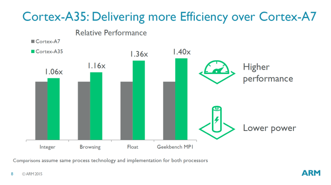
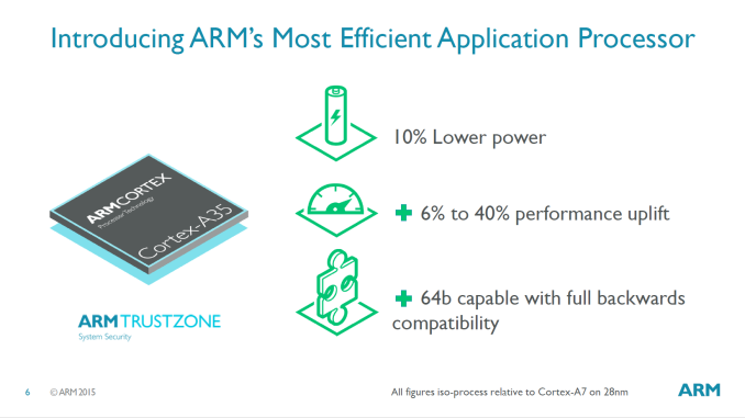
At
the same frequency and process, the A35 architecture (codenamed
Mercury), promises to be 10% lower power than the A7 while giving an
6-40% performance uplift depending on use-case. In integer workloads
(SPECint2006) the A35 gives about 6% higher throughput than the A7,
while floating point (SPECfp2000) is supposed to give a more substantial
36% increase.
What is probably more interesting are apples-to-apples performance and power comparisons to the A53. Here the A35 actually is extremely intriguing as it is able to match the A53's performance from 80% to up to 100% depending on use-case. Browser workloads are where the A35 will trail behind the most and only be able to provide around 80% of the A53's performance. Integer workloads are quoted at coming in at 84-85% of the Apollo core, while as mentioned earlier, memory-heavy workloads are supposed to be on par with the larger bretheren.
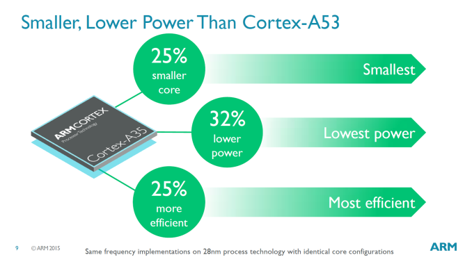
What puts things in perspective though is that the A35 is able to achieve all of this at 75% the core size and 68% the power of the A53. ARM claims that the A35 and A53 may still be used side-by-side and even envisions big.LITTLE A53.A35 designs, but I have a hard time justifying continued usage of the A53 because of the cost incentive for vendors to migrate over to the A35. Even in big.LITTLE with A72 big cores I find it somewhat hard to see why a vendor would choose to continue to use an A53 little cluster while they could theoretically just use a higher clocked A35 to compensate for the performance deficit. Even in the worst-case scenario where the power advantage would be eliminated by running a higher frequency, vendors would still be able to gain from the switch due to the smaller core and subsequent reduced die size.
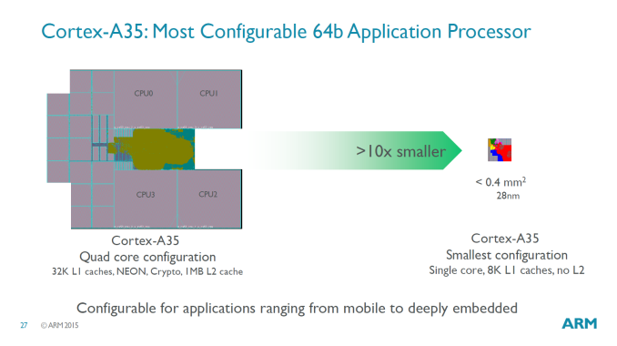
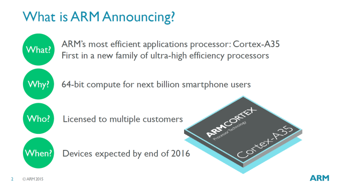
The A35 is touted as ARM's most configurable processor with vendors able to alter their designs far beyond simple choices such the core-count within a cluster. Designers will now also be able to choose whether they want NEON, Crypto, ACP or even the L2 blocks included in their implementations. The company envisions this to be processor for the next billion smartphone users and we'll likely see it in a very large variety of SoCs powering IoT devices such as wearables and embedded platforms, to budget smartphones and even high-end ones in big.LITTLE configurations.
ARM expects first devices with the A35 to ship by the end of 2016. Due to the sheer number of possible applications and expected volume, the Cortex A35 will undoubtedly be a very important CPU core for ARM that will be with us for quite some time to come.
Read More ...
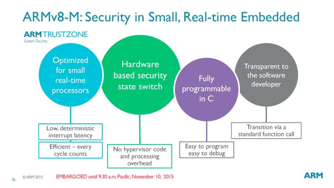
ARM Announces ARMv8-M Instruction Set For Microcontrollers – TrustZone Comes to Cortex-M
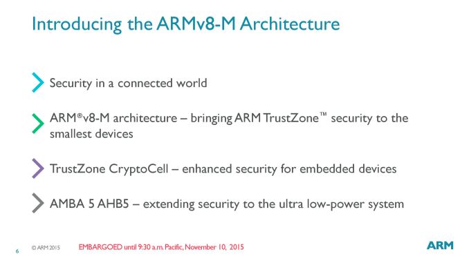
As a brief bit of background since we don’t extensively cover ARM’s microcontroller efforts, in recognition of the unique power and performance requirements for microcontrollers, ARM produces a separate instruction set architecture and lineup of CPU cores specifically for these kinds of products. These are the ARM-M ISAs and the Cortex-M series of CPUs respectively. The ARM-M ISAs can be thought of as a cut-down version of ARM’s full ISAs, paring down the features to allow for simpler CPUs as needed in microcontrollers.
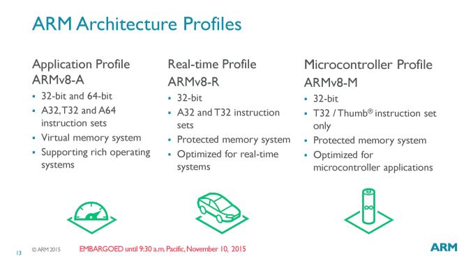
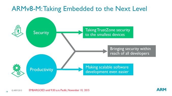
At this year’s TechCon, ARM is announcing the latest iteration of the ARM-M ISA, the ARMv8-M ISA. Unlike the full ARMv8 (i.e. ARMv8-A) ISA that we’re accustomed to seeing implemented in products like ARM’s Cortex-A57 CPU, Apple’s Twister CPU, and other products, ARM’s focus on their microcontroller ISA is a bit narrower. Here the focus isn’t on performance or memory space – factors that led to the expansion to 64-bit CPUs with ARMv8-A AArch64 – but rather on continuing with microcontroller-suitable 32-bit CPUs while investing in the new features ARM sees as important over the next half decade or so.
To that end, ARM’s big focus with ARMv8-M is on security. Key to that is that ARM’s TrustZone technology is coming to microcontrollers for the first time.
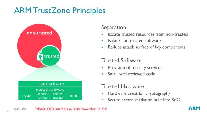
Previously only available to ARM-A architecture CPUs, TrustZone is now being extended to ARM based microcontrollers. And like their bigger siblings, ARM’s aim here with TrustZone is to lay the groundwork for their customers to build highly secure devices, for all the benefits and drawbacks such a device entails. This includes protecting cryptography engines and certain stored assets (e.g. the secure enclave) against attack, locking down systems to prevent userland applications from breaking into the operating system itself, and various degrees of DRM (one example, as ARM gives is, is firmware IP protection).
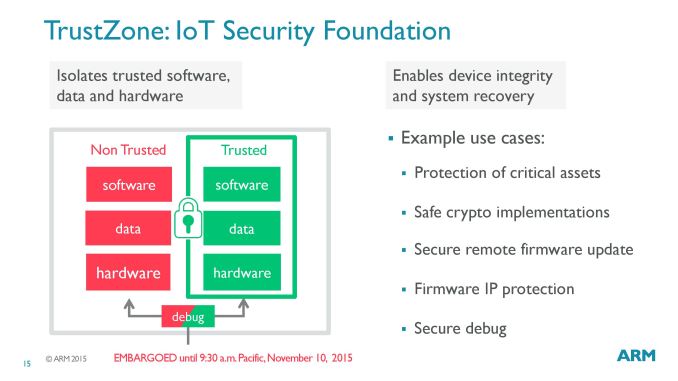
ARM over the last few years has been betting increasingly heavy on wearables and ioT, so the announcement of ARMv8-M and their focus on TrustZone is consistent with those bets. ARM microcontrollers are used in a number of devices as the sole processor, and in more devices still as a specialized processor working alongside a full ARMv8-A application processor. So as ARM microcontroller use increasingly expands from industrial devices and simple black boxes to complex devices that end-users interact with, there is a need for better security to follow into these products.
With that said, as microcontrollers are the lowest of the low power devices in the ARM ecosystem, ARM had needed to take some care in implementing that security within the constraints of a microprocessor. Seeking to avoid compromising response time or efficiency, the ARMv8-M TrustZone retains the deterministic properties developers need on such devices, so a TruzeZone interrupt has a low and deterministic latency to the operation. Similarly, the core of the implementation is based on switching states rather than hypervisors, avoiding the overhead and higher resource requirements of the latter.
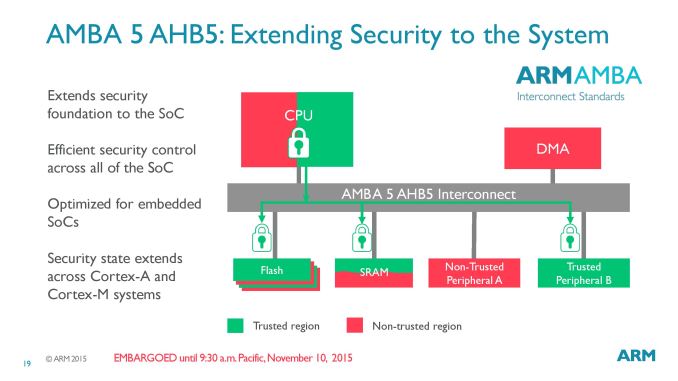
Of course like the ARMv8-M ISA itself, TrustZone is an ISA and a model for just the CPU. To flesh out the full technology ARM is also making a couple of other ARMv8-M announcements. The first is that the company is announcing the ARM Advanced Microcontroller Bus Architecture 5 (AMBA 5) Advanced High-performance Bus 5 (AHB5) specification. The main system bus for ARM’s microcontrollers, AHB5 goes hand-in-hand with TrustZone to extend the security model to the rest of the SoC. Through AHB5, TrustZone microcontroller CPUs can interact with both trusted and non-trusted devices, including trusted segments of SRAM and flash memory as required for implementing separated storage.
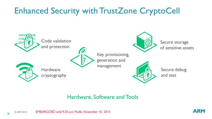
Also being announced today is TrustZone CryptoCell, ARM’s implementation of a TrustZone crypto block, which provides the fixed function hardware necessary for a full TrustZone implementation. The TrustZone CryptoCell includes a secure enclave, key generation/provisioning/management, and the actual fixed function hardware crypto engines.
Ultimately with today’s ARMv8-M and associated security announcements, ARM is looking to further flesh out the ARM ecosystem to support full security at every level and every device from end to end. ARM believes that developers now need an easier and more standardized way to implement security on their microcontroller-equipped devices, and this is what ARMv8-M will provide.
Finally, and not all that surprising, today’s announcement of the ARMv8-M ISA is just for the ISA itself, and not for any specific CPUs. ARM has traditionally announced new Cortex CPU designs separately from the ISA, and in this case it’s no different. To that end ARM isn’t specifically talking about when we’ll see ARMv8-M Cortex-M designs announced, but after today’s announcement it’s safe to say that it’s only a matter of time.


Read More ...
Google Begins Offline Maps Rollout on Android


The feature works in a fairly straightforward manner. When searching a location in maps there will now be a download button in the information page about that location. You can then scroll around to fit the parts of the map you need into the box shown on screen, and when you name and save it the maps for that area will be permanently stored on your device. The applications for this feature are fairly obvious, such as storing maps of areas where you won't have a cell signal, or of places you'll be travelling to in other countries where your phone won't work.
The new version of Google Maps with offline maps is rolling out now on Android, and an updated version for iOS will be coming in the near future.
Read More ...
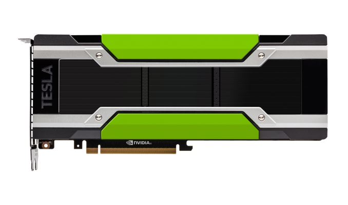
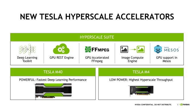
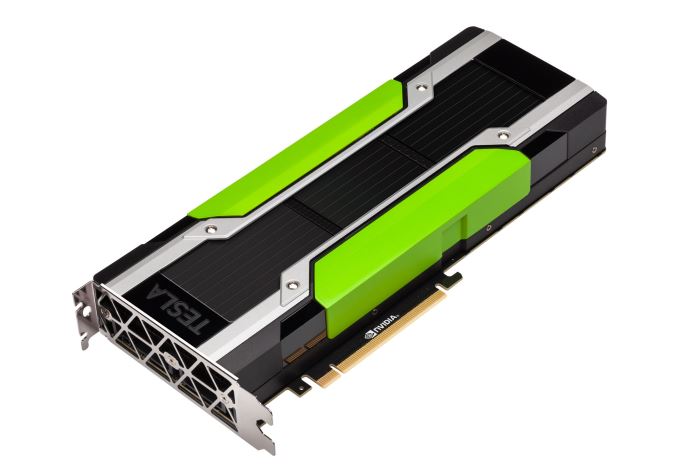
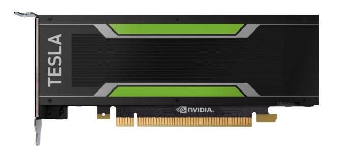
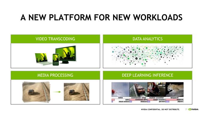
NVIDIA Announces Tesla M40 & M4 Server Cards - Data Center Machine Learning
After August’s announcement of the Tesla M60 and M6 cards – with a focus on VDI and video encoding – NVIDIA is back today for the announcement of the next set of Tesla cards, the M40 and the M4. In what the company is dubbing their “hyperscale accelerators,” NVIDIA is launching these two cards with a focus on capturing a larger portion of the machine learning market.
| NVIDIA Tesla Family Specification Comparison | ||||||
| Tesla M40 | Tesla M4 | Tesla M60 | Tesla K40 | |||
| Stream Processors | 3072 | 1024 | 2 x 2048 (4096) |
2880 | ||
| Boost Clock(s) | ~1140MHz | ~1075MHz | ~1180MHz | 810MHz, 875MHz | ||
| Memory Clock | 6GHz GDDR5 | 5.5GHz GDDR5 | 5GHz GDDR5 | 6GHz GDDR5 | ||
| Memory Bus Width | 384-bit | 128-bit | 2 x 256-bit | 384-bit | ||
| VRAM | 12GB | 4GB | 2 x 8GB (16GB) |
12GB | ||
| Single Precision (FP32) | 7 TFLOPS | 2.2 TFLOPS | 9.7 TFLOPS | 4.29 TFLOPS | ||
| Double Precision (FP64) | 0.21 TFLOPS (1/32) | 0.07 TFLOPS (1/32) | 0.3 TFLOPS (1/32) | 1.43 TFLOPS (1/3) | ||
| Transistor Count | 8B | 2.94B | 2x 5.2B | 7.1B | ||
| TDP | 250W | 50W-75W | 225W-300W | 235W | ||
| Cooling | Passive | Passive (Low Profile) |
Active/Passive | Active/Passive | ||
| Manufacturing Process | TSMC 28nm | TSMC 28nm | TSMC 28nm | TSMC 28nm | ||
| GPU | GM200 | GM206 | GM204 | GK110 | ||
| Target Market | Machine Learning | Machine Learning | VDI | Compute | ||
First let’s quickly talk about the cards themselves. The Tesla M40 marks the introduction of the GM200 GPU to the Tesla lineup, with NVIDIA looking to put their best single precision (FP32) GPU to good use. This is a 250 Watt full power and fully enabled GM200 card – though with Maxwell this distinction loses some meaning – with NVIDIA outfitting the card with 12GB of GDDR5 VRAM clocked at 6GHz. We know that Maxwell doesn’t support on-chip ECC for the RAM and caches, but it’s not clear at this time whether soft-ECC is supported for the VRAM. Otherwise, with the exception of the change in coolers this card is a spitting image of the consumer GeForce GTX Titan X.
Joining the Tesla M40 is the Tesla M4. As hinted at by its single-digit product number, the M4 is a small, low powered card. In fact this is the first Tesla card to be released in a PCIe half-height low profile form factor, with NVIDIA specifically aiming for dense clusters of these cards. Tesla M4 is based on GM206 – this being the GPU’s first use in a Tesla product as well – and is paired with 4GB of GDDR5 clocked at 5GHz. NVIDIA offers multiple power/performance configurations of the M4 depending on server owner’s needs, ranging from 50W to 75W, with the highest power mode rated to deliver up to 2.2TFLOPS of FP32 performance.
Both the Tesla M40 and M4 are being pitched at the machine learning market, which has been a strong focus for NVIDIA since the very start of the year. The company believes that machine learning is the next great frontier for GPUs, capitalizing on neural net research that has shown GPUs to be capable of both quickly training and quickly executing neural nets. Neural nets in turn are increasingly being used as more efficient means for companies to process vast amounts of audio & video data (e.g. the Facebooks of the world).
To that end we have seen the company focus on machine learning in the automotive sector with products such as the Drive PX system and lay out their long-term plans for machine learning with the forthcoming Pascal architecture at GTC 2015. In the interim then we have the Tesla M40 and Tesla M4 for building machine learning setups with NVIDIA’s current-generation architecture.
Given their performance and power profiles, Tesla M40 and M4 are intended to split the machine learning market on the basis of training versus execution The powerful M40 being well-suited for quicker training of neural nets and other systems, while the more compact M4 is well-suited for dense clusters of systems actually executing various machine learning tasks. Note that it’s interesting that NVIDIA is pitching the M40 and not the more powerful M60 for training tasks; as NVIDIA briefly discussed among their long-term plans at GTC 2015, current training algorithms don’t scale very well beyond a couple of GPUs, so users are better off with a couple top-tier GM200 GPUs than a larger array of densely packed GM204 GPUs. As a result the M40 occupies an interesting position as the company’s top Tesla card for machine learning tasks that aren’t trivially scalable to many GPUs.
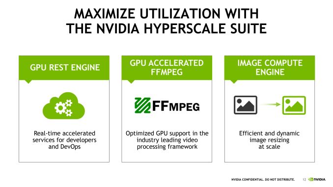
Meanwhile, along with today’s hardware announcement NVIDIA is also announcing a new software suite to tie together their hyperscale ambitions. Dubbed the “NVIDIA Hyperscale Suite,” the company is putting together software targeted at end-user facing web services. Arguably the lynchpin of the suite is NVIDIA’s GPU REST Engine, a service for RESTful APIs to utilize the GPU, and in turn allowing web services to easily access GPU resources. NVIDIA anticipates the GPU REST Engine enabling everything from search acceleration to image classification, and to start things off they are providing the NVIDIA Image Compute Engine, a REST-capable service for GPU image resizing. Meanwhile the company is also be providing their cuDNN neural net software as part of the suite, and versions of FFmpeg with support for NVIDIA’s hardware video encode and decode blocks to speed up video processing and transcoding.
Wrapping things up, as is common with Tesla product releases, today’s announcements will predate the hardware itself by a bit. NVIDIA tells us that the Tesla M40 and the hyperscale software suite will be available later this year (with just over a month and a half remaining). Meanwhile the Tesla M4 will be released in Q1 of 2016. NVIDIA has not announced card pricing at this time.


Read More ...
The Microsoft Surface Book Review
Microsoft has released what they are calling "The Ultimate Laptop" and with their first attempt at moving outside the tablet segment, we take a look at the new Surface Book and how it compares. Competition in the notebook segment is much more intense than the high end tablet market, and Microsoft is aiming for the top.
Read More ...
Imagination Announces New P6600, M6200, M6250 Warrior CPUs
Warrior P6600
Starting off with the P6600, this is Imagination's new MIPS flagship core succeeding the P5600. The P5600 was a 3-wide out-of-order design with a pipeline depth of up to 16 stages. The P6600 keeps most of the predecessor's characteristics such as the main architectural features or full hardware virtualization and security through OmniShield, but adds compatibility for MIPS64 64-bit processing on top. Imagination first introduced a mobile oritented 64-bit MIPS CPU back with the I6400 a little more than a year ago but we've yet to see vendors announce products with it.
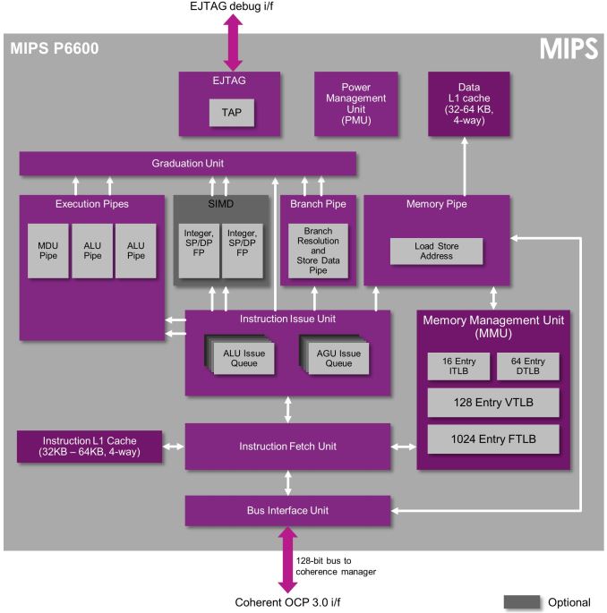
We're still lacking any details on the architectural improvements of the P6600 over the P5600 so it seems that for now we're left with guessing what kind of performance the new core will bring. The P5600 was directly competing with ARM's Cortex A15 in terms of IPC, but ARM has since then not only announced but also seen silicon with two successor IPs to the A15 (A57 and A72), so the P6600 will have some tough competition ahead of itself once it arrives in products.
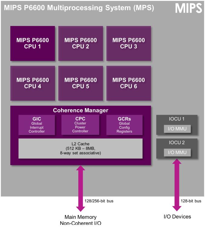
The P6600, much like the P5600 can be implemented from single-core to six-core cluster configurations. What is interesting that as opposed to ARM CPU IP, the MIPS cores allow for asynchronous clock planes between the individual cores if the vendors wishes to implement the SoC's power management in this way (It can also be set up to work in a synchronous way).
"MIPS P6600 is the next evolution of the high-end MIPS P-class family and builds on the 32-bit P5600 CPU. P6600 is a balanced CPU for mainstream/high-performance computing, enabling powerful multicore 64-bit SoCs with optimal area efficiency for applications in segments including mobile, home entertainment, networking, automotive, HPC or servers, and more. Customers have already licensed the P6600 for applications including high-performance computing and advanced image and vision systems."
Warrior M6200 & M6250
Also as part of today's announcement we see two new embedded CPU cores, the M6200 and M6250. Both cores are successors to the microAptiv-UP and UC but able to run at up to 30% higher frequency. The new processors also see an ISA upgrade to MIPS32 Release 6 instead of Release 5.
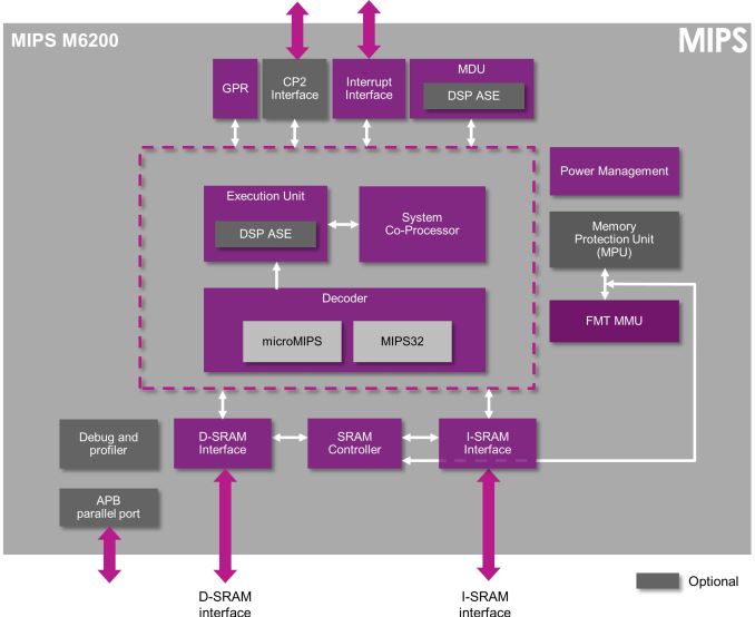
The M6200 is targeted at real-time embedded operating systems with minimal funtionality for cost- and power-savings. It has no MMU and as such can only be described as a microcontroller part.
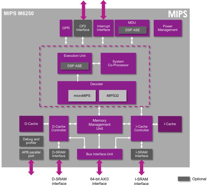
The M6250 is the bigger brother of the M6200 and the biggest difference is the inclusion of a memory management unit (MMU) that makes this a full fledged processor core that can run operating systems like Linux.
"M6200 and M6250 are configurable and fully synthesizable solutions for devices requiring a high level of performance efficiency and small silicon area including wireless or wired modems, GPU supervisors, flash and SSD controllers, industrial and motor control, advanced audio and more."
Read More ...
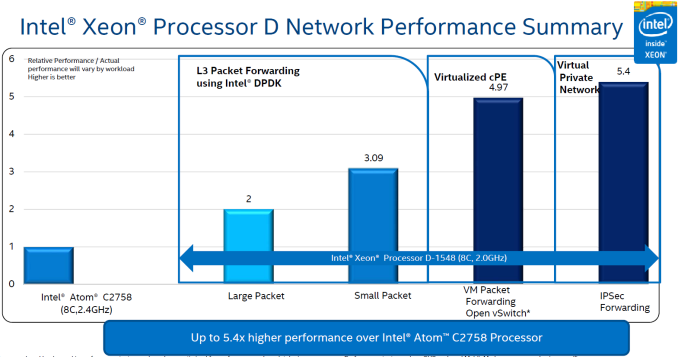
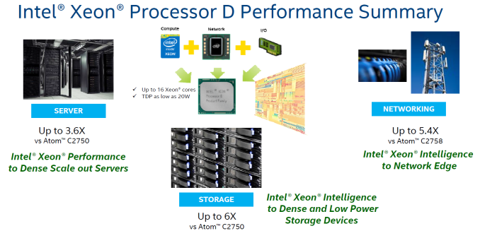
Intel's Xeon D Product Family Updated with Storage and Networking-Specific SKUs
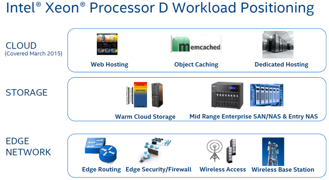
Xeon D was launched with two SKUs (D1520, a 4C/8T SiP, and the D1540, a 8C/16T SiP) earlier this year. While those two SKUs covered the web hosting applications, today's launches cover the storage and edge network applications. Intel's slide from a presentation made earlier today sums up the various products in the lineup. Eight new Xeons and three new Pentium processors are being launched in the D-1500 lineup and they come in both 45W and 35W TDP versions. Interestingly, Intel indicated that 12-core and 16-core Xeon D SiPs can be expected early next year.
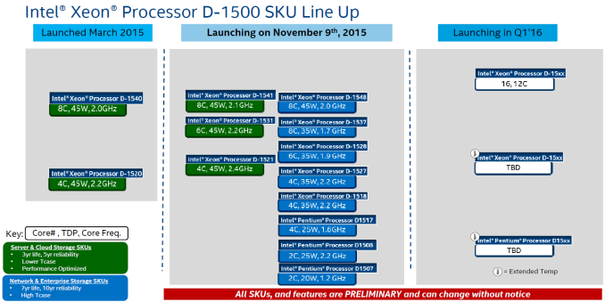
Patrick at ServeTheHome has a nice graphic summarizing the clock speeds and pricing of these products. The D15x1 SKUs target the storage market, while the D15x7 and D15x8 target the networking / communication segments.
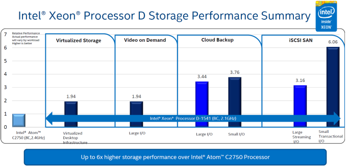
Intel claims that the new storage SKUs provide as much as 6x the performance of the high-end Avoton-based platforms.
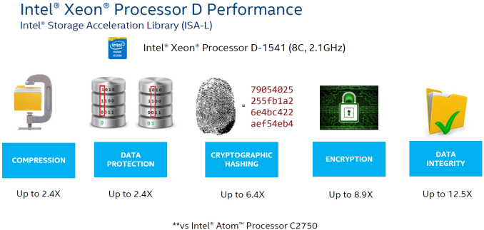
Intel's Storage Acceleration Library (ISA-L) provides accelerators for compression, checksumming, parity calculation and cryptograhic functions (encryption as well as hashing).
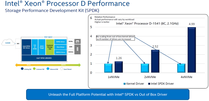
The Storage Performance Development Kit (SPDK) provides better optimization compared to the native Linux drivers - particularly as the number of storage devices in the system ramps up.
On the networking front, Intel claims up to 5.4x higher performance compared to the Rangeley-based platforms. Intel is promoting their Data Plane Development Kit (DPDK) to achieve better performance for L3 packet forwarding, VM packet forwarding with Open vSwitch, and IPSec forwarding (VPN applications).
ServeTheHome talks about how the communication accelerators have gained extensive software support since they were launched with the Rangeley SoCs in 2013.
One of the disappointing aspects with respect to the D1520 and D1540 (at least for those intending to use them as virtualization hosts) was the pulling back of the advertised SR-IOV feature. It remains to be seen if the new SKUs have the feature enabled.
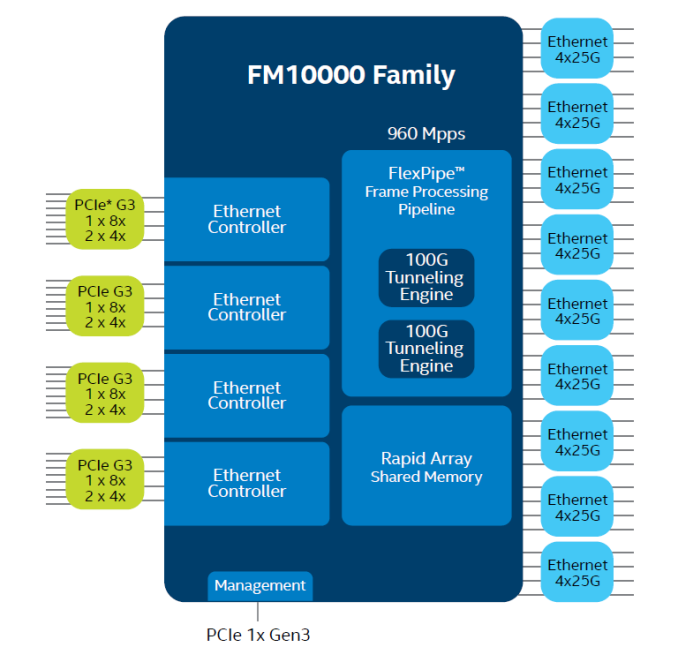
In addition to the new Xeon D SKUs, Intel also announced the FM10000 Ethernet multi-host controller family that can provide up to 36 Ethernet lanes. The FM10000 family supports 1Gbps, 2.5Gbps, 10Gbps, and 25Gbps Ethernet ports and the ability to group four lanes as 40Gbps or 100Gbps ports. The integrated Ethernet controllers can be configured as four 50Gbps or eight 25Gbps host interfaces,.
The new X550 single-chip, low-cost 10GbE platform was also launched. It supports NBASE-T technology (for 2.5Gbps as well as 5 Gbps operation, in addition to 10Gbps).
Operating via a PCIe 3.0 x1 / x4 / x8 link, the new 10GBASE-T controller integrates both MAC and PHY in a single package, and comes in both single and dual-port varieties. Power consumption is just 11 W with both 10GbE ports active, making it amenable to passive heatsink thermal solutions.
Read More ...
TAG Heuer Unveils The Intel-Powered Connected Smartwatch
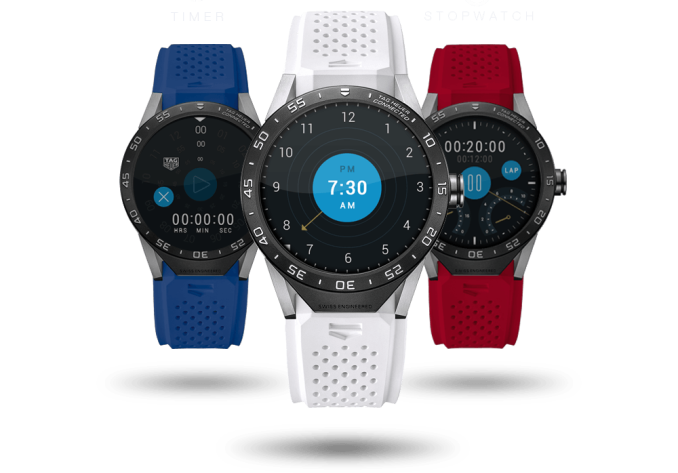
The TAG Heuer Connected has a diameter of 46mm, a thickness of 12.8mm, and a mass of 52 grams. The chassis of the watch is made of titanium, and the LCD display is covered by a sheet of sapphire glass. The display itself is a 1.5" 360x360 fully circular transflective LTPS LCD, which means it can use the reflection of light to improve visibility and drive down power consumption. The last time I remember hearing about these sorts of displays was Pixel Qi's transflective LCDs, but the tech hasn't really gone anywhere since that time. It'll be interesting to see who is making the panel for the TAG Heuer Connected and how it fares in bright light compared to other smartwatches, as well as compared to a traditional mechanical watch which doesn't use an LCD at all.
| TAG Heuer Connected | |
| SoC | Intel Atom Z34xx |
| RAM | 1GB |
| NAND | 4GB |
| Display | 1.5" 360x360 LCD, 240ppi |
| Diameter / Mass | 46mm / 52g |
| Battery | 410mAh |
| OS | Android Wear |
| Other Connectivity | 802.11b/g/n + BT 4.1 |
| Price | $1499 |
Interestingly, the TAG Heuer connect is powered by an Intel SoC rather than the Snapdragon 400 chip that has shown up in most Android Wear devices. More specifically, it's an Intel Z34xx series SoC, which has a peak frequency of 1.6GHz but TAG Heuer notes that the nominal frequency will be more like 500MHz. The SoC is paired with 1GB of RAM and 4GB of NAND, which puts it ahead of the 512MB of RAM found in most Android Wear watches. The sensors include an accelerometer and a gyroscope, but no heart rate monitor which is definitely a letdown for fitness-oriented buyers. The watch is also advertised as having IP67 water resistance.
Because 30% of the Connected's parts are made outside of Switzerland the watch isn't officially "Swiss made", and I don't expect that's going to be an easy problem to overcome when there are now many electrical parts inside the watch being made overseas. Something interesting is that the Connected is modeled off of TAG Heuer's Carrera mechanical watch, and after two years the company will allow you to trade in your Connected along with $1500 to receive an actual Carrera. To me that move seems a bit pessimistic about the company's own future in the smartwatch space, as it seems like there's an assumption that users will give up a smartwatch and go back to owning a mechanical watch. It would make more sense to me if you could trade up to newer versions of the Connected.
The last, and possibly most important detail about the TAG Heuer Connected is the price. TAG Heuer's mechanical watches can cost several hundred dollars, and so it's no surprise that the TAG Heuer Connected will have a retail price of $1500
Read More ...
The Google Nexus 5X Review
Google's first hardware collaboration with LG brought us the Nexus 4. Like the Nexus 7, the Nexus 4 followed a philosophy of bringing as much power and quality as possible to a reasonably affordable price point. The Nexus 4 definitely wasn't a perfect phone, but it was certainly good relative to its price, and it showed that a phone can still be good even if it doesn't cost $600. About one year later Google and LG collaborated again to bring us the Nexus 5, a device which I and many other users fondly remember as an affordable phone that actually brought many of the specifications you would expect to see in a device that costed significantly more.
While I'm sure many hoped that 2014 would bring the next iteration of an LG Nexus device, it wasn't meant to be. Instead we got the Nexus 6 made by Motorola, which didn't really follow the pricing philosophy of the LG Nexus devices, and wasn't very competitive with devices like the Galaxy Note 4 despite its equivalent cost. At that point the future of affordable Nexus devices was unclear, and I wasn't even sure if we'd see a true successor to the Nexus 5. Fortunately, this year is the year that LG returns to bring us the next iteration of their Nexus phones, with the new device appropriately being named the Nexus 5X. Read on for the full review, and find out if the Nexus 5X is a worthy successor to the Nexus 5.
Read More ...
Examining Intel's New Speed Shift Tech on Skylake: More Responsive Processors
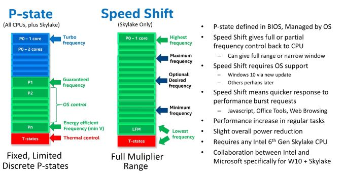
With Skylake, Intel's newest 6th generation Core processors, this changes. The processor has been designed in a way that with the right commands, the OS can hand control of the frequency and voltage back to the processor. Intel is calling this technology 'Speed Shift'. We’ve discussed Speed Shift before in Ian’s Skylake architecture analysis, but despite the in-depth talk from Intel, Speed Shift was noticably absent at the time of the launch of the processors. This is due to one of the requirements for Speed Shift - it requires operating system support to be able to hand over control of the processor performance to the CPU, and Intel had to work with Microsoft in order to get this functionality enabled in Windows 10. As of right now, anyone with a Skylake processor is actually not getting the benefit of the technology, at least right now. A patch will be rolled out in November for Windows 10 which will enable this functionality, but it is worth noting that it will take a while for it to roll out to new Windows 10 purchases.
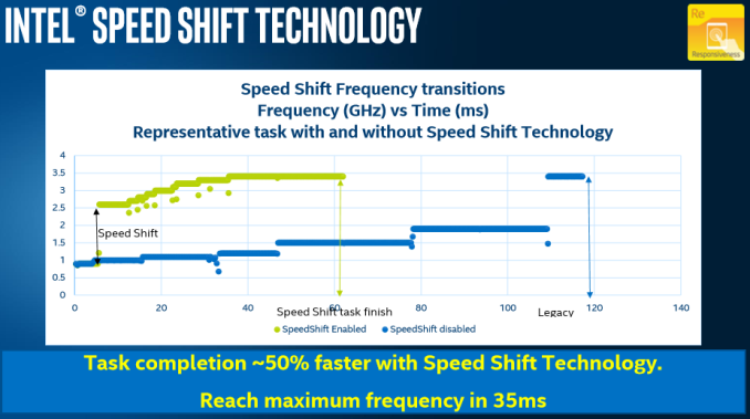
Compared to Speed Step / P-state transitions, Intel's new Speed Shift terminology, changes the game by having the operating system relinquish some or all control of the P-States, and handing that control off to the processor. This has a couple of noticable benefits. First, it is much faster for the processor to control the ramp up and down in frequency, compared to OS control. Second, the processor has much finer control over its states, allowing it to choose the most optimum performance level for a given task, and therefore using less energy as a result. Specific jumps in frequency are reduced to around 1ms with Speed Shift's CPU control from 20-30 ms on OS control, and going from an efficient power state to maximum performance can be done in around 35 ms, compared to around 100 ms with the legacy implementation. As seen in the images below, neither technology can jump from low to high instantly, because to maintain data coherency through frequency/voltage changes there is an element of gradient as data is realigned.
The ability to quickly ramp up performance is done to increase overall responsiveness of the system, rather than linger at lower frequencies waiting for OS to pass commands through a translation layer. Speed Shift cannot increase absolute maximum performance, but on short workloads that require a brief burst of performance, it can make a big difference in how quickly that task gets done. Ultimately, much of what we do falls more into this category, such as web browsing or office work. As an example, web browsing is all about getting the page loaded quickly, and then getting the processor back down to idle.
For this short piece, Intel was able to provide us with the Windows 10 patch for Speed Shift ahead of time, so that we could test and see what kind of gains it can achieve. This gives us a somewhat unique situation, since we can isolate this one variable on a new processor and measure its impact on various workloads.
To test Speed Shift, I’ve chosen several tasks which have workloads that could show some gain from Speed Shift. Tests which run the processor at its maximum frequency for long periods of time are not going to show any significant gain, since you are not limited by the responsiveness of the processor in those cases. The first test is PCMark 8, which is a benchmark which attempts to represent real-life tasks, and the workload is not constant. In addition, I’ve run the system through several Javascript tests, which are the best case scenario for something like Speed Shift, since the processor has to quickly complete a task in order to allow you to enjoy a website.
The processor in question is an Intel Core i7-6600U, with a base frequency of 2.6 GHz, and turbo frequency of 3.4 GHz. Despite the base frequency being rated on the box at 2.6 GHz, the processor can go all the way down to 400 Mhz when idle, so being able to ramp up quickly could make a big impact even on the U-series Skylake processors. My guess is that it will be even more beneficial to the Y series Core m3/m5/m7 parts since they have a larger dynamic range, and typically more thermal constraints.
PCMark 8
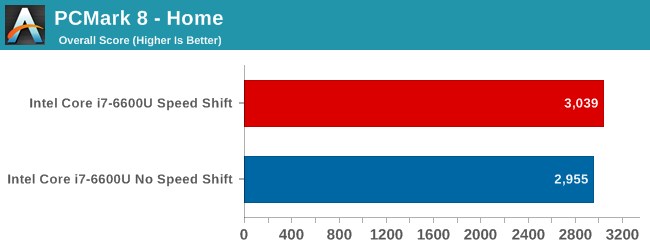
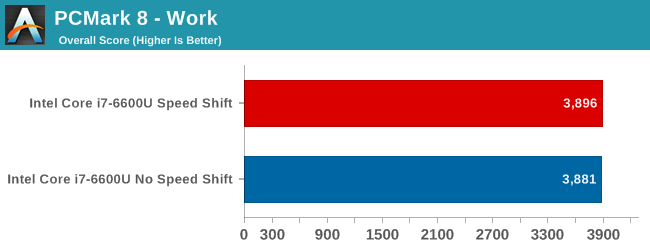
Both the Home and Work tests show a very small gain with Speed Shift enabled. The length of these benchmarks, which are between 30 and 50 minutes, would likely mask any gains on short workloads. I think this illustrates that Speed Shift is just one more tool, and not a holy grail for performance. The gain on Home is just under 3%, and the difference on the Work test is negligible.
JavaScript Tests
JavaScript is one of the use cases where short burst workloads are the name of the game, and here Speed Shift has a much bigger impact. All tests were done with the Microsoft Edge browser.
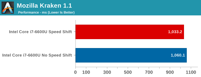

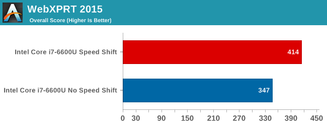
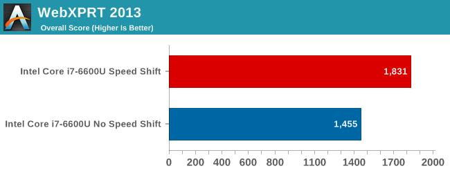
The time to complete the Kraken 1.1 test is the least affected, with just a 2.6% performance gain, but Octane's scores shows over a 4% increase. The big win here though is WebXPRT. WebXPRT includes subtests, and in particular the Photo Enhancement subtest can see up to a 50% improvement in performance. This bumps the scores up significantly, with WebXPRT 2015 showing an almost 20% score increase, and WebXPRT 2013 has a 26% gain. These leaps in performance are certainly the kind that would be noticeable to the end user manipulating photographs in something like Picasa or watching web-page based graph adjustments such as live stock feeds.
Power Consumption
The other side of the coin is power consumption. Having a processor that can quickly ramp up to its maximum frequency could mean that it will consume more power due to the greater penalty of increasing the voltage, but if it can complete the task quickly and get back to idle again, there is a chance to be more efficient when work is done in 10s of milliseconds rather than 100s of milliseconds, as the frequency ramps up and down again before the old P-state method has decided to do anything. The principle of 'work fast, finish now' was the backbone of Intel's 'Race To Sleep' strategy during the ultrabook era and focused on the impulse of response-related performance, however the drive for battery life means that efficiency has tended to matter more, especially as devices and batteries get smaller.
Due to the way modern processors work, we don’t have the tools to directly measure the SoC power. Intel has told us that Speed Shift does not impact battery life very much, one way or the other, so to verify this, I've run our light battery life test with the option disabled and enabled.
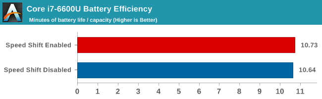
This task is likely one of the best case scenarios for Speed Shift. It consists of launching four web pages per minute, with plenty of idle time in between. Although Speed Shift seems to have a slight edge, it is very small and would fall within the margin of error on this test. Some tasks may see a slight improvement in efficiency, and others may see a slight regression, but Speed Shift is less of a power savings tool than other pieces of Skylake. Looking at it another way, if, for example, the XPS 13 with Skylake was to get 15 hours of battery life, Speed Shift would only change the result by about 7 minutes. Responsiveness increases, but net power use remains about the same.
Final Words
With Skylake, while there was not the large leap in clock for clock performance gain that we have become accustomed to with new Intel microarchitectures, but when you look at the overall package, there was a decent net gain in performance combined with new technologies. For example, being able to maintain higher Turbo frequencies on multiple cores has increased the stock to stock performance more than the smaller IPC gains.
Speed Shift is just one small part of the overall performance gain, and one that we have not been able to look at until now. It does lead to some pretty big gains in task completion, if the workloads are bursty and short enough for it to make a difference. It can’t increase the absolute performance of the processor, but it can get it to maximum performance in a much shorter amount of time, as well as get it back down to idle quicker. Intel is billing it as improved responsiveness, and it’s pretty clear that they have achieved that.
The one missing link is operating system support. We’ve been told that the patch to enable this is coming to Windows 10 in November. While this short piece looks at what Speed Shift can bring to the table in terms of performance, if you'd like to read more about how it is implemented, please check out the Skylake architecture analysis which goes into more detail.
Update: Daniel Rubino at Windows Central has tested the latest Windows 10 Insider build 10586 and it appears to enable Speed Shift on his Surface Pro 4, which is in-line with the November timeline we were provided.
Read More ...
Jumbo Joust: iPad Pro vs. Surface Pro 3 vs. Surface Pro 4
May the best oversized tablet win
Read More ...
Twitter Senior VP: "Diversity is Important, But We Can’t Lower the Bar"
Twitter's (supposedly) last black manager unloads accusations against his former employer; numbers seem to corroborate his account
Read More ...
"Prepare to be Punished": Microsoft is Killing OneDrive With Cuts, Blames Users
OneDrive went from promising to pathetic in one day flat
Read More ...
BlackBerry Priv is an Amazing Android So Secure You May Never Hear of It
Shockingly BlackBerry has produced one of the best available Android devices, but so far AT&T is the only U.S. carrier to commit to it
Read More ...
True Beef or Sloppy Sausage? Digging Into the Red Meat + Cancer Correlation
A recent study used meta-analysis to determine that meat is a carcinogen -- but how much danger are we really in?
Read More ...
Lenovo Whoa: Motorola Droid MAXX 2 and Turbo 2 Break Cover in Leaks
Droid MAXX 2 will target the mid-range while Turbo 2 will be the flagship variant
Read More ...
Leak: Apple Preps for First Real Android App Foray With New Apple Music App
App is expected to drop within the next month, appears to support all the same features that iOS users enjoy
Read More ...
Sony Again Doubles Down on Smartphones, Eyes Cost Cuts w/ New Thailand Plant
Plant will manufacture millions of high-end Xperias per year and will be wholly owned by Sony; meanwhile financial losses continue
Read More ...
Ford, Toyota, and Universal Pictures Celebrate "Back to the Future Day' in Style
Back to the Future Pt. II proves both prophetic and nostalgic in retorspect -- and some companies are eager to tap into this mojo
Read More ...
Consumer Reports Flexes Muscle, Hits Slumping Tesla Motors Stock
Tesla also has been struck with accusations of roughing up reporters at its gigafactory and by suggestions that the Model X is too pricey
Read More ...
Debunked: Beneath the Lies, Nigerian "Pee Generator" Is Still Pissing Into the Wind
Hydrogen doesn't grow on trees... well not free hydrogen gas, at least
Read More ...
Quick Note: Whoops, Microsoft Pushed Unwanted Windows 10 to Some Users
"Glitch" caused checkbox to default to enabled in Windows 7/8/8.1 causing some to be given an unexpected gift of Windows 10
Read More ...
CNN Resorts to Internet Censorship to Promote Clinton Over Senator Sanders
Meanwhile Sen. Paul continues to face similar attacks from the media, which is accused of favoring Trump
Read More ...
Apple's New "Magic" Peripheral Line Packs High Tech, High Prices
Scissor Keys, Force Touch, Li-Ion Batteries make their way into the peripherals
Read More ...
Quick Note: Windows 10 Insider Preview Build 10565 Fixes Boot Camp 6.0 Issues
New build tunes up Windows 10 into fine form
Read More ...
Pepsi Smartphone? Empty Calories Coming Soon to the Midrange
Device spec isn't bad, but the CPU listing is curious given that it labels a clearly non-64-bit MediaTek chip as a 64-bit SoC
Read More ...
Legere Blasts Microsoft for "Bull***t" Snub of T-Mobile and Verizon
Microsoft's pitch to carriers has been apathetic if reports are to be believed; AT&T favoritism allegedly lives on
Read More ...
Microsoft Band 2 Stays Focused on Fitness, Debuts Oct. 30, Priced at $249
Wearable integrates Cortana but manages to avoid distraction of becoming too much of a smartwatch
Read More ...
Microsoft's HD-500 ("Display Dock"), the Magic Sauce Behind Continuum
Propietary hardware will be required for now; price not announced; device support will be limited initially to new models
Read More ...
Quick Note: Windows 10 Hits 110 Million Devices, VMs
Microsoft is seeing roughly 7.5 million free upgrades and/or new device purchases per week
Read More ...
Microsoft Lumia 950 and 950 XL Finally Launch, w/ Windows 10, Liquid Cooling
Also onboard is 20 MP camera, microSD, triple-LED flash, a Qualcomm Snapdragon 810 SoC, Iris Scanner, USB 3.1, and an adaptive antenna
Read More ...
Why the U.S. Won't be Able to Ban Google's New Huawei Marshmallow Flagship Phone
(and other asssorted thoughts on the launch of Android Marshmallow (6.0) and the Nexus 5X and 6P devices)
Read More ...
Tag Heuer Admits Its $1,800 Smartwatch Was Inspired By Apple -- Price-Wise
New premium smartwatch will vie with the Apple-Hermes alliance for the luxury crow
Read More ...
Apple's First Fixes to iOS 9 Land w/ iOS 9.0.1 Release
Release comes remarkably early as Apple tries a new strategy to buck the bug blues
Read More ...
Breaking Bad: How to Crash Google's Chrome Browser With Just 8 Characters
It's not just the 'a' one that's been floating around
Read More ...
Apple Watch Commands 2 in 3 Smart Watch Sales, WatchOS 2 Sweetens the Pitch
Expanding availability portends bullish holiday sales of Apple's wearable
Read More ...
Ghost in the Machine: Apple, Developers Unwittingly Aid App Store Malware
Tens, if not hundreds of thousands of non-jailbroken devices are believed infected after a Trojan compiler malware struck in China
Read More ...
Worth the Wait? Microsoft Teases at Windows 10 Flagship Phones to Air Oct. 6
Surface Pro 4 and Band 2 waerable are also expected to be announced, alongside the new flagship Lumia 950 (or 940?) and 950 XL
Read More ...
Fakebook Pt. I: From "The Chive" to "AskMen"; How Facebook's Phonies are Born and Used
Shady promotion, sex trafficking, and data mining are just some of the tricks of the trade for Facebook's growing population of fakers
Read More ...
Available Tags:ASUS , Android , NVIDIA , Tablet , Tablet , AMD , Catalyst , CPU , Google , Server , Microsoft , Xeon , iPad , Twitter , BlackBerry , Lenovo , Motorola , Apple , Apple , Sony , Windows , Windows , Windows , Windows , iOS , iOS , Chrome , Windows ,
No comments:
Post a Comment