
The ASUS Z170-A Motherboard Review: The $165 Focal Point
In the world of technology, you could speculate if there is ever a golden age, or a renaissance. All the time we expect technology to grow and improve, being better than the last. Sometimes there is nostalgia, but it never stops us using the latest because it provides the user experience we expect at a minimum. Like all the motherboard manufacturers, I've followed ASUS for years, and observed their constant iteration as platforms evolve. The newest Skylake platform is upon us, and we review the ASUS Z170-A motherboard to see their interpretation of the desktop this generation.
Read More ...
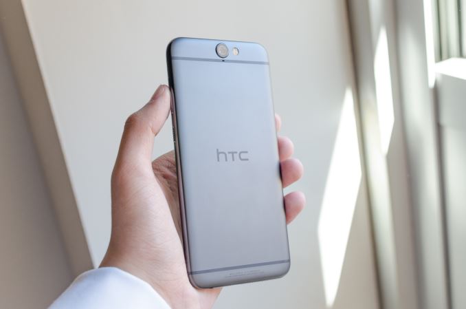
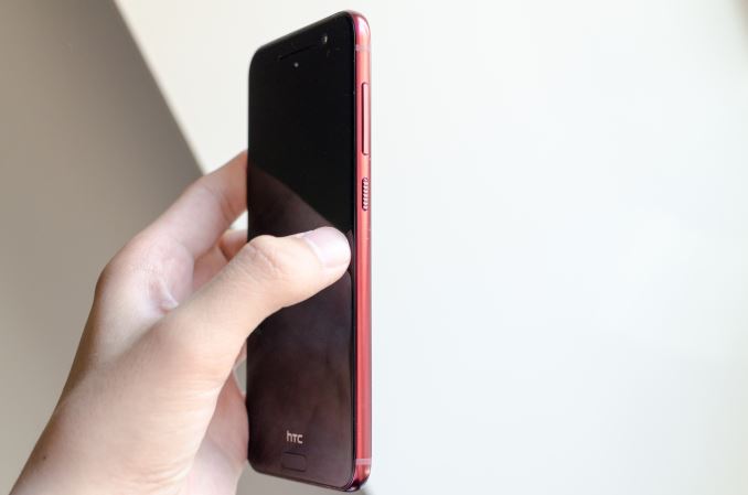
Hands On With the HTC One A9
| HTC One A9 | |
| SoC | Qualcomm MSM8952 Snapdragon 617 4 x Cortex A53 @ 1,5GHz 4 x Cortex A53 @ 1.2GHz |
| GPU | Adreno 405 |
| RAM | 2/3GB LPDDR3 |
| NAND | 16/32GB + microSDXC |
| Display | 5.0" 1920x1080 AMOLED |
| Dimensions | 145.75 x 70.8. x 7.26 mm, 143g |
| Camera | 13MP Rear Facing with F/2.0 aperture + OIS 4MP UltraPixel Front Facing with F/2.0 aperture |
| Battery | 2150mAh (8.17Wh) |
| OS | Android 6.0 Marshmallow with HTC Sense |
| Cellular Connectivity | 2G / 3G / 4G LTE (Qualcomm X8 Category 7 LTE) |
| Other Connectivity | 2.4/5GHz 802.11a/b/g/n/ac + BT 4.1, GNSS, microUSB 2.0 |
| SIM | NanoSIM |
| Price | $399 |
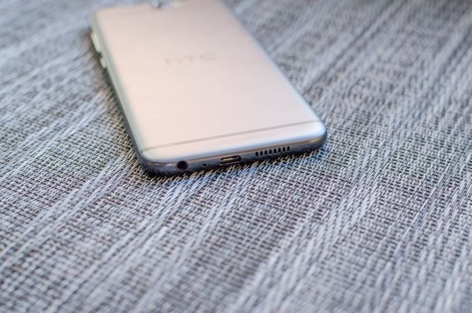
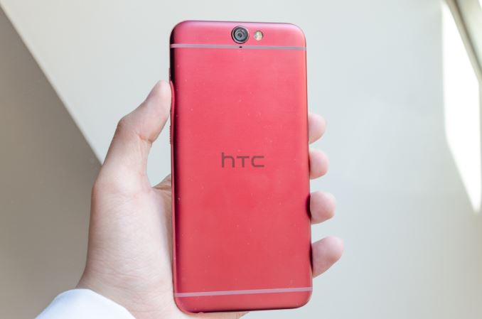
In some ways, HTC is really an outlier with the release of this phone. For the most part this year I’ve seen OEM after OEM releasing phones that are either uncomfortable or basically impossible to use with one hand with the rare exception of the Galaxy S6. In fact, the One A9 is almost identical to the Galaxy S6 in height and width, but is roughly half a millimeter thicker. However, the One A9 is noticeably thinner in the hand by virtue of a more rounded transition to the back of the phone.
Since we’re talking about the form of the phone, it’s probably obvious by now that this phone bears at least a passing resemblance to an iPhone 6 or 6s. HTC claims that this design isn’t designed to ape the iPhone, and in some ways they are correct as the antenna design is noticeably different when directly compared to the iPhone 6 and 6s. The sides of the phone are also curved differently and reminiscent of the Desire 800 series as the sides of the phone have a much less aggressive radius of curvature than what is seen in recent iPhones. These sides are also relatively glossy instead of the coarser sand-blasted finish seen on the iPhone.
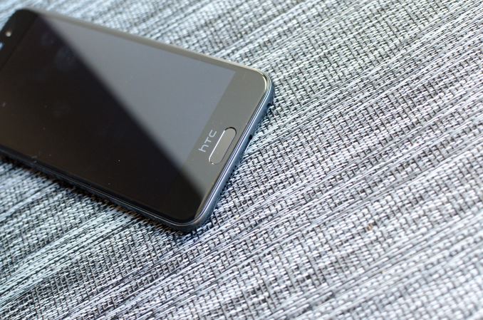
In some ways, the comparisons seem unavoidable. From the front of the phone, the design doesn’t really look like a Desire smartphone due to the all glass design. The earpiece is also a departure from recent HTC designs, although HTC has used such a design before with the EVO LTE. The fingerprint scanner was seen as recent as the One M9+, but at the time it was partially shared with the speaker grille instead of part of the glass. The glass is also a 2.5D curved piece so edge swipes are smooth, which is something we saw with the One X but hasn’t made a return until now.

These are all design elements that we’ve seen in HTC phones before, but the sum results in a phone that looks a bit too close to the iPhone 6 for comfort. In practice, it does feel like a very different phone than the iPhone 6, but when only looking at photos it’s probably hard to tell that this is the case. If I were to look at previous HTC smartphones, I do see a strong resemblance to the One S, but the design of the One S is still quite different from what we see in the One A9. Regardless of whether this is an iPhone-inspired design or not, the design is a breath of fresh air after multiple launches of 5.5” size phones with ever-increasing size.
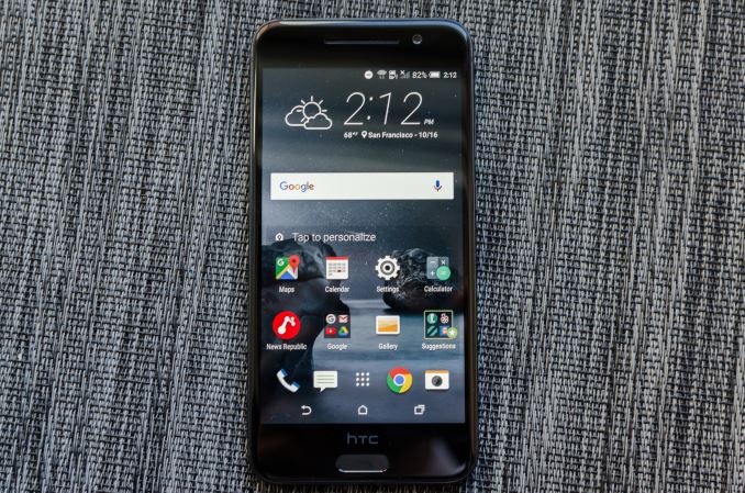
Putting design aside, there are some other major departures in this phone for HTC. The first is that this is a return to an AMOLED display, in the form of a 1080p AMOLED display. I wasn’t able to determine whether this is equivalent to the Galaxy S5 or S6 generation of AMOLED but the display gives a noticeably blue reflection when the screen is off when compared to the Galaxy S6 and S5, which could be indicative of what generation AMOLED technology we’re dealing with. Interestingly enough, HTC has included a display setting to toggle between “AMOLED” and sRGB mode, which could bode well for those that care about color accuracy in displays.
The SoC is also not exactly the definition of high-end, as HTC has elected to use a Snapdragon 617 which is likely due to issues with the Snapdragon 810 and 808. As far as I can tell Snapdragon 618 or 620 weren’t possible at this time so it seems that HTC is in some ways stuck between a rock and a hard place when it comes to SoC choice. In some ways, I don’t really see another choice here, especially given the price point that HTC is competing in. The SoC platform choice also means battery PMICs and handshake ICs with support for Qualcomm’s QC 3.0 quick charge standard.
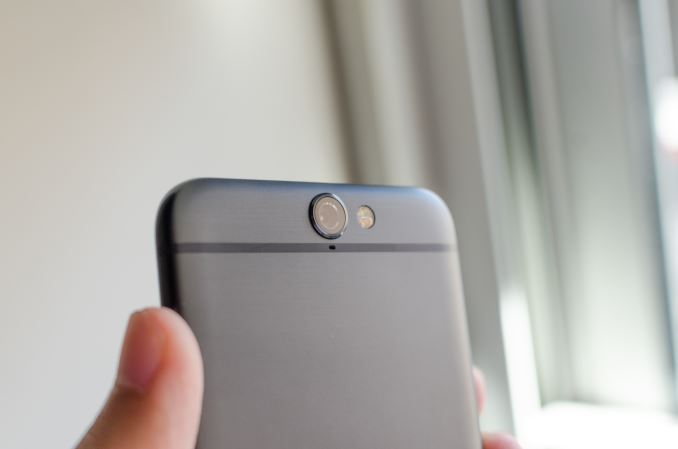
The camera is arguably one of the major notable points for HTC here, as it’s a 13MP IMX214 sensor with F/2.0 optics and second generation OIS. This sounds kind of boring at first glance but taking some quick relative comparison shots indoors with the iPhone 6 and Galaxy S6 for comparison was shocking to see when the One A9 was comparable, if not even better than the Galaxy S6 in the dimly lit room in which I tried the One A9. There’s also a feature that allows for automatic processing of RAW photos on the phone, which is impressive but processing a single photo took a significant amount of time relative to the near-instant output of normal photos. I would estimate that a single photo took as long as 10-20 seconds to process, which suggests that a better SoC would go a long way towards improving the UX here.
The fingerprint sensor is also surprisingly fast and accurate in my experience, and noticeably improved over the One M9+. HTC emphasized that this was necessary for a good Android Pay experience, which means that this phone also has NFC which appears to work off of the top metal antenna but lacks the boosting system seen in the iPhone 6 so NFC behavior is going to be similar to other HTC phones.
The software experience is also notably changed when compared to the One M9. Although many parts of the phone are still going to look like the same HTC Sense that we’ve seen since the start of this year, other parts like the notification drawer, camera app UI, multitasking menu, and the removal of a number of HTC Sense apps like the HTC Music and Internet apps and the HTC Calendar widget. I personally think HTC may have taken out too many HTC apps and widgets here, but the updates to make HTC Sense fit better with Material Design is definitely a good thing.

On the audio side, HTC is claiming that Dolby Audio enhancement and 24-bit 192 KHz will dramatically improve audio quality. I didn’t get a chance to test these claims, but the headphone jack does use an RT5506 amplifier from the One M8 which had great audio quality from our testing. The speaker also has a TFA9895 amp on it which should help with quality but due to the downward-firing nature of this speaker the quality is likely to be worse than what we saw on the One M8.
Overall, while this isn’t the holiday season flagship that some might be expecting, I came away quite impressed with this phone. Despite the mid-range SoC I was more impressed with this phone than the One M9 at launch. Obviously, the true successor to the One M9 is the phone that everyone is really waiting on, but this phone shows that HTC is capable of responding to clear market demands. Although not every piece of the A9 is what I’d want to see in the M10, aspects like the dramatically improved camera processing, renewed focus on industrial design, and changes to HTC Sense should definitely be carried over.
The HTC One A9 will be offered in Opal Silver, Carbon Gray, and Deep Garnet starting at 399.99 USD unlocked with 3GB of RAM and 32GB of storage. One variant will support Sprint, while the other will support T-Mobile, AT&T, and Verizon with a pre-activated SIM. HTC will also offer their Uh-Oh protection for phones sold through HTC.com, which means 12 months of coverage for accidental damage from drops or water damage with one free replacement, along with a 6 month subscription to Google Play Music.
Read More ...
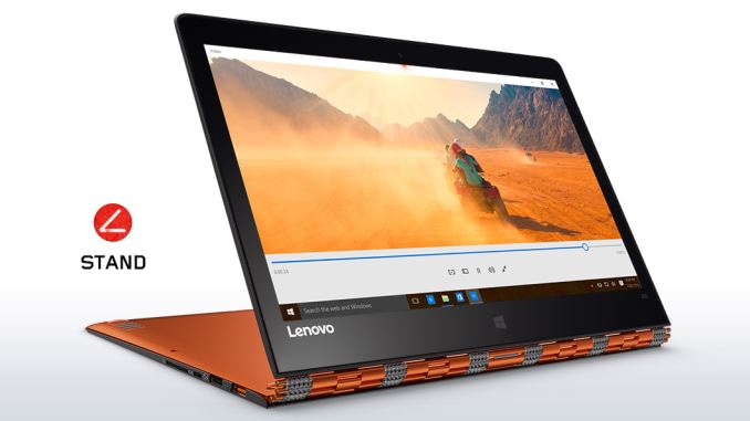
The Lenovo Yoga 900 Series Launched: The ‘Thinnest’ Core Laptop and a 27-inch Portable All-In-One
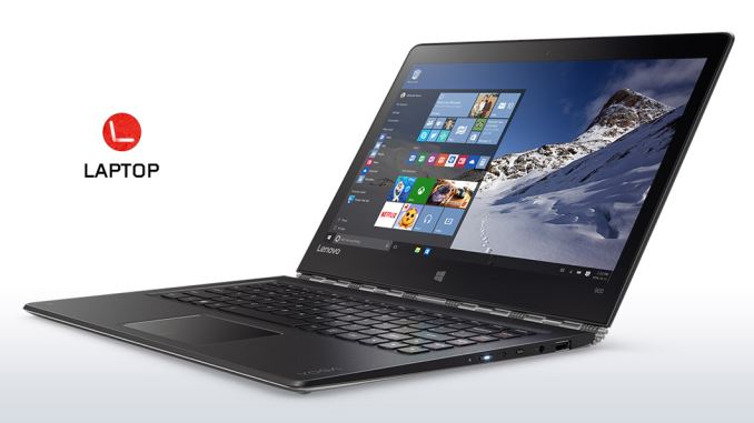
Lenovo Yoga 900
| Lenovo Yoga Specifications | ||||||
| Yoga 2 Pro | Yoga 3 Pro | Yoga 900 | ||||
| Processor | Intel Core i3-4010U (15W) Intel Core i5-4200U (15W) Intel Core i7-4500U (15W) |
Intel Core M-5Y71 (4.5W) | Intel Core i7-6500U (15W) | |||
| Memory | 4-8GB DDR3L-1600 | 8GB DDR3L-1600 | 8-16GB DDR3L-1600 | |||
| Graphics | Intel HD 4400 (20 EUs, Gen 7.5) |
Intel HD 5300 (24 EUs, Gen 8) |
Intel HD 520 (24 EUs, Gen 9) |
|||
| Display | 13.3" Glossy IPS 16:9 QHD+ (3200x1800) |
13.3" Glossy IPS 16:9 QHD+ (3200x1800) LCD |
13.3" Glossy IPS 16:9 QHD+ (3200x1800) LED |
|||
| Hard Drive(s) | 128GB/256GB/512GB SSD (Samsung mSATA) |
256GB/512GB SSD (Samsung PM851) |
256GB/512GB SSD (Samsung ?) | |||
| Networking | Intel Wireless-N 7260 (2x2:1 802.11n) |
Broadcom 802.11ac (2x2:2 802.11ac) |
Intel Wireless AC-8260 (2x2:2 802.11ac) | |||
| Audio | Realtek HD Stereo Speakers Headset jack |
JBL Stereo Speakers 1.5w x 2 Headset jack |
JBL Stereo Speakers Dolby® DS 1.0 Headset jack |
|||
| Battery | 4 cell 55Wh 65W Max AC Adapter |
4 cell 44Wh 40W Max AC Adapter |
4 cell 66Wh | |||
| Buttons/Ports | Battery status indicator Novo button 1 x USB 2.0 1 x USB 3.0 Headset Jack Volume Screen Rotation Lock AC Power Connection 1 x Micro-HDMI SD Card Reader |
Power Button Novo Button 2 x USB 3.0 Headset Jack Volume Control Auto Rotate Control DC In with USB 2.0 Port 1 x Micro-HDMI SD Card Reader |
Power Button 2 x USB 3.0-A 1 x USB 3.0-C Headset Jack SD Card Reader DC In with USB 3.0-A Port |
|||
| Back Side | Exhaust vent | Watchband Hinge with 360° Rotation Air Vents Integral to Hinge |
||||
| Dimensions | 12.99" x 8.66" x 0.61" 330 x 220 x 15.5 mm |
13" x 9" x 0.5" 330.2 x 228.6 x 12.8 mm |
12.75" x 8.86" x 0.59" 324 x 225 x 14.9 mm |
|||
| Weight | 3.06 lbs (1.39 kg) | 2.6 lbs (1.18kg) | 2.8 lbs (1.3 kg) | |||
| Extras | 720p HD Webcam Backlit Keyboard |
|||||
| Colors | Silver Grey Clementine Orange |
Light Silver Clementine Orange Golden |
Platinum Silver Clementine Orange Champagne Gold |
|||
| Pricing | $879 (256GB) $1049 (512GB) |
$1148 (256GB) $1379 (512GB) |
$1200 (8GB/256GB) $1300 (8GB/512GB) $1400 (16GB/512GB) |
|||
With Intel’s 6th Generation, as most OEMs will be moving to, Lenovo is hoping to leverage new features such as Speed Shift and video decode to improve both performance and battery life. Over the previous generation of Yoga laptops, the Yoga 900 comes in a little heavier than the Yoga 3 Pro but allows up to 16GB of memory, comes immediately with Windows 10 Home and also sports a USB Type-C 3.0 with video out functionality. Currently all versions listed online come with the i7-6500U, one of the top Skylake Core i7 15W models with GT2 integrated graphics. Lenovo is listing the battery life as nine hours of local video playback, as well as sporting a 50% increase in battery density.


Prices start at $1200 for the 8GB/256GB version, rising to $1400 for 16GB/512GB models. There will be versions in Lenovo’s Clementine Orange, but also Platinum Silver and Champagne Gold. From looking at the breakdown online, not all colors will be available in all specifications.
Lenovo Yoga Home 900
Cast your minds back to 2014. It was a fun time, with Haswell and Broadwell processors from Intel being talked about as bringing a revolution to the mobile computing market. I remember some of the product ideas becoming quite amusing at the time, especially when Intel was talking about making all-in-one devices (where the PC built into the monitor and you just add a keyboard/mouse) something that could be carried around. Clearly something that measures up to 32-inches in this context is going to be heavy and short on battery life, and was perhaps not something to be taken too seriously as a product idea. Fast forward to the end of 2015, and Lenovo is going to sell you one.

Information about the specifications is small right now, but we are told that at 27-inches, the device will come with a 5th generation processor, Windows 10 and offer up to three hours of battery life. The 5th generation processor part is interesting, suggesting a Broadwell part – if this is a 47W or 65W processor, it could be an eDRAM equipped processor in that instance. Nevertheless there will probably be a range available, as Lenovo is going to offer the Yoga Home 900 with optional NVIDIA GeForce 940A graphics as well. The software package from Lenovo will include the AURA 3.0 interface which allows for image manipulation and a selection of apps from the Windows Store developed with portable AIOs in mind.


Prices for the Lenovo Yoga Home 900 will start at $1549 and be available from the end of October.
Source: Lenovo
Read More ...
ARM Announces Mali-470 GPU: Low Power For Wearables & More
Though chasing the low-end of the market doesn’t come with the glamour of the high-end (and for that there’s Midgard), for ARM it has in many ways the textbook low-price/high-volume success story. The company’s estimates put them in plenty of low-end tablets and smartphones, but more unexpectedly they have a lion’s share of the smart TV market, with 75% of TVs implementing a Mali design. With TVs only requiring enough graphics power for basic UI functions and video decoding at 1080p – few smart TVs play games or do fancy transparency/animation effects – even after having been eclipsed by more powerful GPUs at the high-end, the Mali-400 family has found a second home in these sort of simple devices that need little more than a no-frills GPU, be it for cost reasons, power reasons, or both.
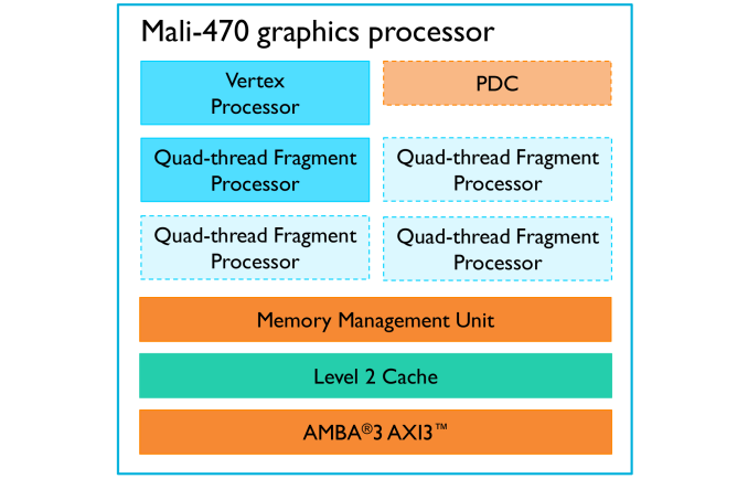
Given the continued success of the Mali-400 family it should come as little surprise then that ARM has continued to develop the family, as the need for OpenGL ES 2.0 won’t be coming to an end any time soon. To that end, today ARM is announcing the release of the next iteration of the Mali-400 family IP, the Mali-470. Mali-470 serves as something of a decedent of both Mali-400 and Mali-450, with ARM intending to make it a direct successor to Mali-400 while also integrating some of the improvements that original went in to Mali-450 as well.
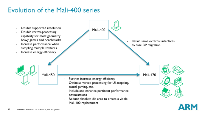
With the Mali-470 ARM is specifically targeting the IoT and embedded market, even more so than they were already going after it with the Mali-400 and Mali-450. In recent times the Mali-450 has been ARM’s more powerful Mali-400 family GPU, specifically going after low-end devices and the aforementioned TV market. Meanwhile thanks in part to the introduction of smaller processes since its introduction in 2008, the Mali-400 has already been something of a darling for low-power applications, appearing in wearable devices such as Samsung’s Gear S2. ARM and their licensees continue to be bullish on wearables and IoT in general, and this has lead to ARM setting out to develop a more direct update to the Mali-400 to further improve on its energy efficiency.
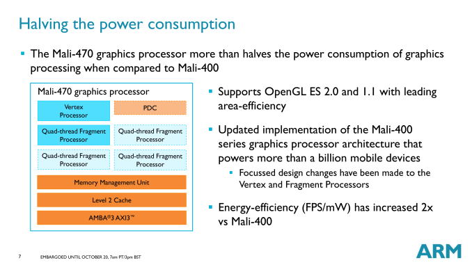
Overall ARM is aiming to double Mali-400’s energy efficiency with Mali-470, in accordance with their goals to reach further into the wearables and IoT market. To do so, ARM has taken some of Mali-450’s energy optimizations and further built on them; chief among these changes are far more extensive use of power gating to shut off transistors when they’re not needed, and improved use of clock gating when power gating isn’t an option. In order to accomplish this ARM has implemented separate power domains on Mali-470 – each pixel/fragment block can be on its own domain – and working with these domains is an on-GPU power controller, which works with the system power controller to better manage the GPU.
Improving the use of power and clock gating can greatly impact overall energy efficiency by cutting down on the amount of energy wasted by the GPU waiting for its next job, but it’s especially potent for bringing down idle power consumption. In turn, given that idle power consumption continues to be one of the chief issues dogging wearables vis-a-vis battery life, the Mali-470 should help out battery life to a degree thanks to these improvements.
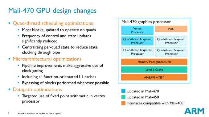
Along with these immediate power optimizations, ARM has also made some smaller optimizations to the Mali-400 family architecture to cut down on wasted power at a workload level. Mali-470’s vertex processor has been optimized to better handle fixed-point arithmetic, a use case that is again very common in simple UIs and can be even more power efficient than floating-point arithmetic. The pixel/fragment processor on the other hand has not gone untouched, with ARM working to cut down on the amount of time spent by the fragment processors changing between states.
| ARM Mali-400 Family | |||||
| 400 | 450 | 470 | |||
| Fragment Shader Blocks (MP#) | 1-4 | 1-8 | 1-4 | ||
| Vertex Shader Blocks | 1 | 1 | 1 | ||
| Architecture | Utgard | Utgard | Utgard | ||
| OpenGL ES | ES 2.0 | ES 2.0 | ES 2.0 | ||
| Year Released (IP) | 2008 | 2012 | 2015 | ||
Moving on, in terms of scalability Mali-470 retains the multi-processor capabilities of the previous Mali designs, allowing Mali-470 to be scaled up from 1 fragment processor (MP1) to as many as 4 (MP4). Mali-470MP1 will in turn be the intended design for wearables given its spot as the lowest-power design, while the more powerful designs will allow Mali-470 to be used in other environments where more performance is needed. That ARM would retain their scalability for Mali-470 is a very intentional choice; as we mentioned earlier Mali-470 is intended to be the successor to Mali-400, with ARM going so far as to keep Mali-400’s MMU and bus interfaces and holding Mali-470’s die area closer to Mali-400’s. This in turn means that Mali-470 needs to be able to carry on from where Mali-400 has left off, not only in the wearables/IoT market but in the embedded market as well.
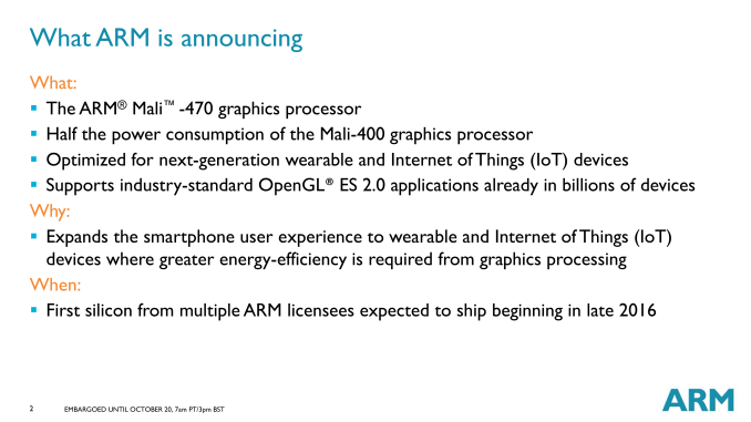
Wrapping things up, as with past ARM IP launches today’s announcement coincides with the general release of new IP to ARM’s customers. ARM tells us that they expect chips integrating Mali-470 designs to start leaving the fabs in the second-half of 2016, which would in turn have Mali-470 start appearing in consumer devices in the first-half of 2017. Ultiamtely ARM doesn’t control which products use which IP, but given their intentions with Mali-470, there’s a good chance that those consumer devices will include Android/Tizen wearables launching early that year.


Read More ...
More Greenlow Motherboards Announced: ASRock Rack’s C230 Series
C236 WS
First up is the full ATX model, giving support for dual PCIe co-processors at PCIe 3.0 x8/x8, dual Intel networking (I210 and I219), another PCIe 3.0 x4 slot from the chipset, a total of eight SATA ports with SATA Express in there as well, an onboard USB 3.0 Type-A port and eight other USB 3.0 ports through two headers and a four ports on the rear panel.
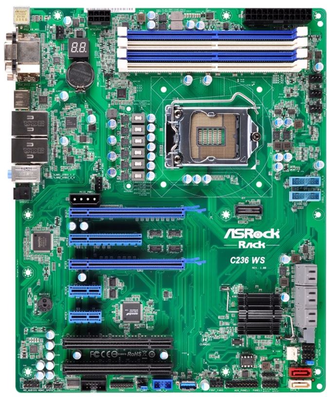
Compared to the consumer ASRock motherboards, this is eminently more clinical and aimed at its specific market – there is low end onboard audio (ALC662 or lower), COM and TPM support, display outputs and PCIe to PCI bridges for legacy connections.
C236M WS (link)
The micro-ATX member of this family carries over a number of features, such as the dual networking (this time I219-LM and I210) and eight SATA ports, but also implements an M.2 connector and a SATA DOM. Audio is boosted up to at least the ALC892 with 5.1 support, and the power delivery on the processor gets a heatsink for good measure. Perhaps surprisingly we see a total of six fan headers as well.
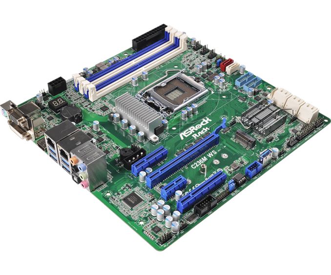
Despite the layout of the PCIe slots, the bottom open-ended x8 is part of the CPU lanes, offering x8/x8 configuration with a PCIe 3.0 x4 at the top from the chipset. Unfortunately, despite the free PCIe lanes in the system, that M.2 slot is only geared for PCIe 3.0 x1 bandwidth.
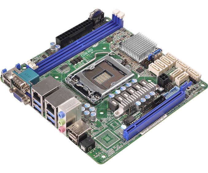
C236 WSI (link)
Similar to the boards from GIGABYTE Server, the smaller mini-ITX one is the more interesting out of the set. Here’s a small board with support for up to 32GB of ECC DDR4 memory, a total of eight SATA ports, dual network controllers (again I219 and I210), a full PCIe 3.0 x16 and a rear-IO COM header.
There’s an interesting large gap in the bottom left however, showing solder pads but no integrated chip. The size of the pad suggests that there is room here for an Alpine Ridge controller, suggesting that in the future there might be a version with either USB 3.1 or Thunderbolt 3.
Availability of these motherboards will be dependent on B2B distribution channels, although we might see one or two filter into commercial channels as well.
Source: ASRock Rack


Read More ...
Skylake Xeon Motherboards: GIGABYTE’s C230 Series Announced
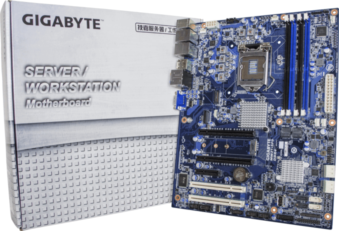
MW31-SP0 (link)
First up is a dual graphics workstation board for SLI or Crossfire with dual Intel network ports (I210+I219-LM), a COM port, TPM support, M.2 support and an interesting proprietary connector between the CPU socket and the PCIe slots for expansion cards:
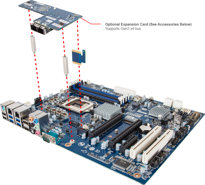
GIGABYTE Server sells cards for 10 gigabit Ethernet, Thunderbolt 3 via Intel’s Alpine Ridge controller, or additional M.2 slots as required. This proprietary connector has bandwidth for up to four PCIe lanes, and the range of cards that will be offered will most likely depend on the take-up of this connector and how many customers are interested in customizing parts of their motherboard like this.
Other features include an on-board USB Type-A port for software license dongles and the use of a low-end Realtek ALC887 audio codec that we normally find on low end motherboards. Interestingly rather than take the full eight SATA ports from the chipset, here there are four as expected but another four from a Marvell 9230 controller, which does not support RST but its own control storage system for RAID. The PCIe x4 slot in the middle of the motherboard is only a PCIe x2 by design, and we also get USB 3.0 support via a VLI controller rather than the chipset. There is no IMPI control on this motherboard either.
MW21-SE0 (link)
Moving to micro-ATX, this model is somewhat stripped out providing a base entry into a Skylake Xeon workstation. There is no onboard audio for example, only a single PCIe 3.0 x16, only one Intel I219-LM network controller, a TPM, some SATA ports and USB headers, plus four DDR4 slots for up to 64GB of memory. Add in a COM port, VGA for the AST1400 control and that’s about it.

The design is offers a four-phase processor arrangement, with the final PCIe slot at x4 from the chipset. Despite the image above looking as if the DDR4 memory is inserted sequentially, it seems that this ‘stock’ photograph is from a mockup where the slots were placed in the wrong colors.
MX11-PC0 (link)
On the server side, the MX11-PC0 actually looks like an interesting mini-ITX motherboard for the rest of the ecosystem to consider. It somewhat attempts to adhere to the thin mini-ITX standard with a half-height rear IO, but there are a number of interesting elements to this worth noting. The DRAM slots are positioned for server use, but the power ports are still on the outside of the motherboard in such a way that a couple of features stick out.
First up is the U.2 port, where the battery is stuck to. This uses the SFF-8639 connector which we’ve seen on Intel’s SSD 750, and runs at PCIe 3.0 x4 speeds with NVMe support. We’ve seen this connector on a couple of ASUS ROG boards so far (the Impact and Extreme), but the more the merrier. Aside from the PCIe 3.0 x16 slot and SATA ports we also get an AST2400 controller IC with an associated memory chip, and a pair of Intel I210 network ports.

The rear of the board also gets co-locator LED buttons and power/reset/NMI buttons.
MX31-BS0 (link)
In a similar server style, the MX31-BS0 also puts the socket/DRAM orientation more suited for server airflow but also attempts to aim for that low to mid-range implementation with IPMI control via an AST2400, dual I210 network ports, an M.2 slot supporting SATA and PCIe 3.0 x1, onboard USB 2.0 Type-A and what amusingly looks like a Realtek audio codec onboard but the system comes without rear-panel audio jacks, leaving the audio solely for SPDIF output.

Typically motherboards from GIGABYTE’s Server business unit start as B2B sales only and the more consumer focused models should end up on select retailers over the next few months.
Source: GIGABYTE Server


Read More ...
Intel Launches ‘Greenlow’: C236 Chipset and Skylake E3-1200 v5 Xeons
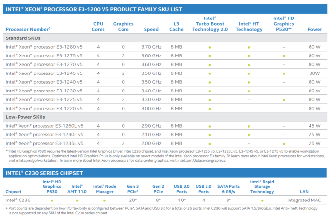
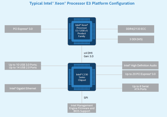
In a somewhat muted launch today, without any PR announcement or anything in the way of details direct, Intel quietly launched details regarding their new workstation single-processor platform based on Skylake. Through Intel’s processor information repository, Intel ARK, eleven socketed models were released in the E3-1200 v5 Xeon family. As with previous Xeons, the goal here is to supply server level features that wouldn’t normally be on consumer grade hardware. All these parts support DDR4 un-buffered modules in both non-ECC and ECC configurations up to 16 GB per module, giving 64 GB maximum. Xeon platforms historically run at base JEDEC memory configurations, so expect to see DDR4-2133 at 15-15-15 subtimings being the norm. Similar to the Skylake consumer parts, DDR3L up to 1600 MT/s is also supported.
These are all quad core parts, ranging from 25W low power models at 2.1 GHz base clock (with hyperthreading) up to up to 80W for the fastest 3.7 GHz model. Prices will range from $193 for the E3-1220 v5 up to $612 for the E3-1280 v5. As shown in the table, only a select few will have integrated graphics, and those that do will be under the HD P530 designation, which if we refer to the standard Skylake launch corresponds to a GT2 configuration with 24 execution units. At this point in time, there are no dual core parts.
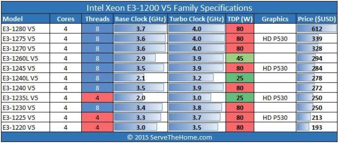
Several parts clearly fly out as interesting – the E3-1275 v5 comes in at just over half the price of the E3-1280 v5 for only a 100 MHz deficit on the base clock. For $9 less, the E3-1270 v5 does the same as the E3-1275 v5 but without the integrated graphics. The one below that, the E3-1260L v5, is one of the low power parts at 45W but still comes close in single threaded frequency to those above it. One of Intel’s big comparison points to these parts will be with Xeon D-1540, also known as Broadwell-DE. This is a 45W part that offers eight cores at 2.0 GHz base/2.6 GHz turbo, with similar DDR4 support but 12MB of L3 cache ‘at $581’.
Users interested in the perennial alternative to the Core processors, the E3-123x range, might come up empty handed this generation. Not necessarily due to the processor itself, but multiple sources in discussion or published at ComputerBase are concluding that Intel is further locking the Xeon processors down for Skylake. This means that in order to use a Xeon processor, you need a server based chipset, such as the C230 series, rather than the 100-series found in consumer platforms. Several companies have confirmed that a ‘workaround’ in this case is most likely not possible.
This new segregation tactic shows that Intel is perhaps trying to adjust any overlap these two markets may have had for non-business users, putting more power into the hands of the OEMs that develop pre-build systems. While E3-1200 based server motherboards have not been difficult to source in the past, they tend to be workstation/server focused and not have bells and whistles that accompany consumer boards. This also removes any thought of potential overclocking that may/may not be overlooked in some Xeon parts in the past. That being said, we have seen ASUS/ASRock release workstation type motherboards in the past that still have consumer trimmings.
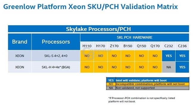
The new Greenlow platform (E3-1200 v5 Xeon plus C232/C236 motherboards) will look like the consumer counterparts with sixteen PCIe lanes for co-processors, dual DDR4/DDR3L memory support, DMI Gen 3.0 to the PCH, a mix of PCIe 3.0 lanes from the chipset, support for up to eight SATA 3.0 ports, and a myriad of possibilities through 26 lanes of HSIO.
At this point in time the launch seems to be biased towards workstations rather than anything 1P server related, but information is currently patchy. At this point in time we are looking to get sampled with some of these processors, along with appropriate motherboards as well. Some motherboard announcements have been made from GIGABYTE Server and ASRock Rack, and I suspect workstation OEMs will come forth in due course.
Source: ComputerBase, ServeTheHome, Intel ARK
Read More ...
ASUS Announces the Z170-based Maximus VIII Extreme ROG Motherboard
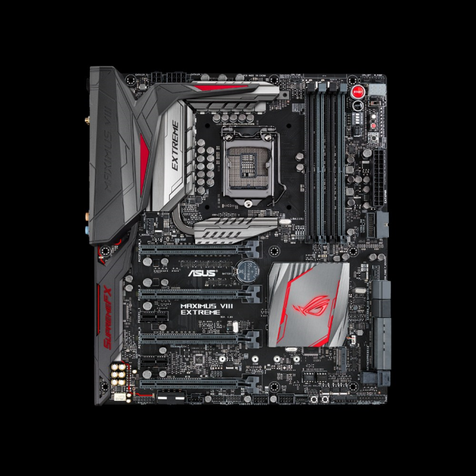
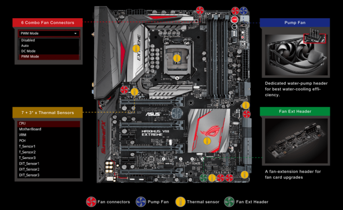
As with most elements of technology, a product can be engineered beyond specification, almost to the point of being a little crazy. High end halo motherboards tend to do this not only to satiate the users who will spend $5000 and up on an extreme system, but to also showcase their engineering talent in a mass market (no one-off chrome Aventadors here). For overclocking this means for the M8E (Maximus VIII Extreme) power delivery that is both quick to react and capable of holding overclocks way beyond normal specifications, DRAM arrangements rated up to DDR4-3866 when all memory slots are populated, enhanced base-clock control to north of 400 MHz, a bundled OC panel with updates for Skylake and extra onboard buttons and switches to help with BIOS selection, updates and memory recovery.
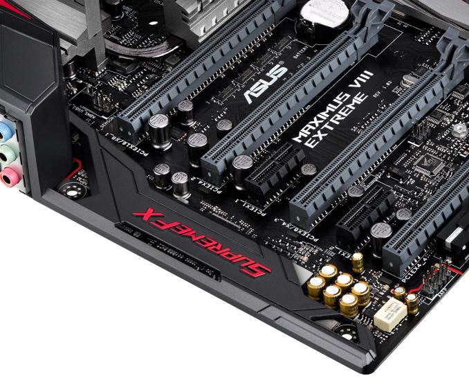
For gamers, the M8E will house ASUS’ latest evolution of their ALC1150 audio solution dubbed SupremeFX 2015. This includes an enhanced DAC, ultra-low-jitter, high-end capacitors and filters, headset impedance detection up to 600 ohms, as well as software features to enhance aspects of gameplay (noise reduction, footsteps, on-screen audio directional locator). The M8E will support ‘quad-SLI’ and ‘quad-CFX’, but only in certain situations – despite looking the part, it is not equipped with a PLX 8747 PCIe switch (that would normally enable the PCIe graphics lanes to be split for up-to x8/x8/x8/x8 operation, which is slowly becoming rarer on mainstream motherboards as the price of this switch has significantly increased over the last two years). Instead ASUS is using an x8/x4/x4 arrangement with another PCIe 3.0 x4 from the chipset, allowing for quad-CFX in x8/x4/x4/x4 mode or quad-SLI when dual-GPU cards are used in the x8/x8 slots. ASUS also equips the M8E with an Intel I219-V network controller with electrostatic protection and software optimization for network traffic prioritization, as well as a tri-stream 3T3R 802.11ac wireless solution.
For software, ASUS is bundling the M8E with updated iterations of RAMCache, KeyBot II and AI Suite, but also new in the bag is Overwolf, a display sub-system that allows for browsing, email, messaging or streaming while in-game.
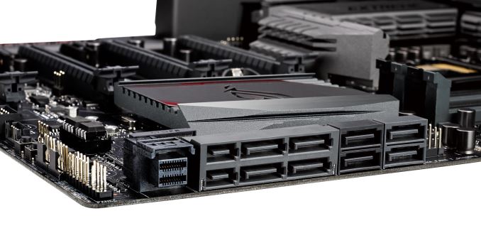
Storage is a big part of the M8E, with U.2 support directly next to the SATA ports for SSD 750 users, SATA Express, M.2 running at PCIe 3.0 x4, and then we also have Thunderbolt 3 alongside USB 3.1 at 10 Gbps both in Type-A and Type-C.
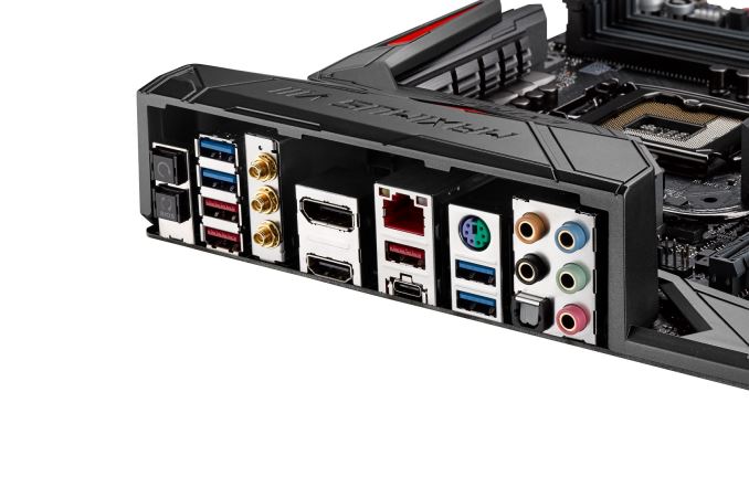
The Thunderbolt 3 support is provided by Intel’s Alpine Ridge controller in a Type-C connector format. This port can also run in USB 3.1 mode, with the AR controller giving two of the USB 3.1 ports (one Type-C and one Type-A). The other two Type-A USB 3.1 ports at 10 Gbps are given by ASMedia’s ASM1142 controller, which we’ve seen on a number of motherboards already.
Perhaps to be expected, the M8E will not be the cheapest board in the market. At $500, and it should be available from today in NA, the Extreme line remains the realm of users with a spare bit of green and the need for a high-end system. It would be interesting to see this paired up against the other $500 motherboard on the market, the GIGABYTE Z170X-Gaming G1, as we already have it in for review.
Source: ASUS


Read More ...
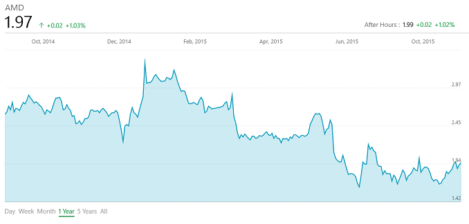
AMD Announces FY 2015 Q3 Results: Decreased Computing And Graphics Sales Hurt Bottom Line
| AMD Q3 2015 Financial Results (GAAP) | |||||
| Q3'2015 | Q2'2015 | Q3'2014 | |||
| Revenue | $1.06B | $942M | $1.43B | ||
| Gross Margin | 23% | 25% | 35% | ||
| Operating Income | -$158M | -$137M | $63M | ||
| Net Income | -$197M | -$181M | $17M | ||
| Earnings Per Share | -$0.25 | -$0.23 | $0.02 | ||
On a Non-GAAP basis, AMD had a $97 million operating loss, which is once again a larger loss than last quarter, and down 211% from the $87 million in operating income last year. Net loss was $136 million, or $0.17 per share, compared to a $41 million net profit and $0.05 per share last year. GAAP to Non-GAAP differences are due to $48 million in restructuring fees and $13 million in stock based compensation.
| AMD Q3 2015 Financial Results (Non-GAAP) | |||||
| Q3'2015 | Q2'2015 | Q3'2014 | |||
| Revenue | $1.06B | $942M | $1.43B | ||
| Gross Margin | 23% | 28% | 35% | ||
| Operating Income | -$97M | -$87M | $87M | ||
| Net Income | -$136M | -$131M | $41M | ||
| Earnings Per Share | -$0.17 | -$0.17 | $0.05 | ||
The Computing and Graphics segment continues to struggle, although AMD did see stronger sequential growth here with the recent launch of Carrizo. Revenue increased 12% over last quarter, although it is still down 46% year-over-year. This segment had an operating loss of $181 million for the quarter, up from a loss of $147 million last quarter and a loss of $17 million a year ago. Sequentially, the loss is mostly attributed to a write-down of $65 million which AMD is taking on older-generation products. Annually, the decrease is due to lower overall sales. Unlike Intel, AMD processors had a decrease in Average Selling Price (ASP) both sequentially and year-over-year, so there was no help there from the lower sales volume. The GPU ASP was a different story, staying flat sequentially and increasing year-over-year. Recent launches of new AMD graphics cards have helped here.
| AMD Q3 2015 Computing and Graphics | |||||
| Q3'2015 | Q2'2015 | Q3'2014 | |||
| Revenue | $424M | $379M | $781M | ||
| Operating Income | -$181M | -$147M | -$17M | ||
The Enterprise, Embedded, and Semi-Custom segment had a better showing. Revenue increased 13% over last quarter, and was down only 2% year-over-year. Semi-custom sales (read Consoles) drove the sequential increase but lower embedded and server processor sales caused a year-over-year decline. Operating income for this segment came in at $84 million, up from $27 million in Q2 but down from $108 million in Q3 2014. Q2’s numbers were skewed though by a $33 million hit on moving to a new process node.
| AMD Q3 2015 Enterprise, Embedded and Semi-Custom | |||||
| Q3'2015 | Q2'2015 | Q3'2014 | |||
| Revenue | $637M | $563M | $648M | ||
| Operating Income | $84M | $27M | $108M | ||
All Other had an operating loss of $61 million for the quarter, up from $17 million loss in Q2 and a $28 million loss in Q3 2014. This is where they stick their “restructuring charges” and they nicely align with the GAAP vs Non-GAAP values.
The bad news doesn’t stop here either. We’ve seen the departure of a couple of key people at AMD, and AMD is also spinning off some of the company. Revenues for Q4 are expected to decrease an additional 10%, plus or minus 3%, compared to today’s numbers. AMD is doing more corporate restructuring in an attempt to reduce expenses further. Perhaps the most troubling aspect of today’s results is their gross margin is only 23%. They really need closer to 35% for profitability and are a long way from that today.
Source: AMD Investor Relations
Read More ...
AMD To Spin-Off Back-End Testing & Assembly Operations Into Joint Venture For $371 Million

Briefly then, in the world of semiconductor manufacturing the complete process of creating a chip is divided into two halves. There is the front-end manufacturing step where a complete wafer of chips is fabbed, and the back-end manufacturing step where those finished wafers are tested and cut up into individual chips for customer use. Dubbed ATMP – for assembly, test, mark, and pack – these back-end operations are in modern times split up from the fabbing step for cost reasons. Consequently capital-intensive and technologically advanced fabbing process will take place in facilities like TSMC Taiwan, GlobalFoundries Germany, and Intel US, while ATMP takes place at facilities in China, Malaysia, and Vietnam.
Up until their spin-off of GlobalFoundries in 2009, AMD had a complete chip manufacturing operation, including facilities for both the fabbing and ATMP operations. Even after the spin-off however, AMD held on to their ATMP operations. It is these operations that AMD is now spinning-off as well, as the company pursues an operations strategy more befitting of a fabless semiconductor designer.
For the deal with NFME, AMD will be spinning-off their ATMP operations into a new, unnamed joint venture in partnership with NFME. The joint venture will see AMD contribute their ATMP facilities in Penang, Malaysia and Suzhou, China, along with their roughly 1,700 person ATMP staff. Meanwhile, though not mentioned in the release, NFME will be contributing their own facilities and employees as well, with the complete joint venture set to have 5,800 employees spread over five facilities.
On the financial side of matters, NFME will immediately be buying an 85% stake of AMD’s ATMP operations, putting NFME in control of the overall joint venture while AMD serves as the minority partner with their remaining 15% share. In turn, NFME will be paying AMD approximately $371 million, and after taxes and other costs this will be a net gain of about $320 million for AMD.
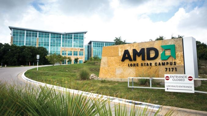
Overall AMD is touting this as a beneficial change for the company, though they also don’t attempt to hide their current financial state in the announcement, stating that the joint venture and sale “further strengthens our balance sheet with significant asset monetization.” AMD on the whole has been struggling with a series of losses over what has now been a number of years, and it has taken a toll on their cash reserves. In the last few years the company has been slowly selling off non-essential or legacy assets in order to both contain ongoing costs and to raise much-needed cash for day-to-day operations. This, among other things, has included selling off and then leasing back their “Lone Star” campus in Austin, Texas.
For AMD, the spin-off means they will be removing 1,700 employees from their payroll, which would put their adjusted headcount at around 7,500 to 8,000 employees after the deal closes. Furthermore as ATMP is capital-intensive, this allows AMD to further contain their spending on capital expenditures. AMD has until now held on to their ATMP operations, and at the time of the GlobalFoundries deal stated that they were keeping these operations as they were specifically tailored to AMD’s microprocessor business. However there’s no doubt that the have been an increasing drag on AMD as the company’s revenues and chip volume have continued to shrink. Ultimately as AMD was already fabless, it’s rare to see a fabless company with their own back-end operations anyhow, and AMD believes they can continue to meet their ATMP needs through this joint venture.
As for the joint venture itself, this gives NFME the ability to further expand into the market for semiconductor assembly and test services (SATS). With AMD’s lower product volumes no doubt making it harder to fully utilize their high-volume AMTP facilities, a joint venture with NFME can bring more work into those facilities by having them work for additional customers beyond AMD. Furthermore NVME also gains the R&D experience that comes with AMD’s AMTP operations, which for them is a competitive advantage against other 3rd party SATS providers.
Ultimately today’s announcement of a joint venture is at best mixed news for AMD. Containing costs is important for the company’s ongoing health and clearly the company no longer has the resources or demand to stay in any kind of manufacturing. On the other hand as the company continues to sell off assets in one form or another – and all the while continues to lose cash as happened again this quarter – it puts them in a perilous position of having to operate off of fewer and fewer assets. So hopefully this joint venture and accompanying sale helps the company focus on the chip and architectural development they need to do, and provide the funding over the next few years to accomplish it.
Read More ...
NVIDIA GeForce Experience Update: 4K GameStream & 1080p Twitch; Driver Update Changes To Come
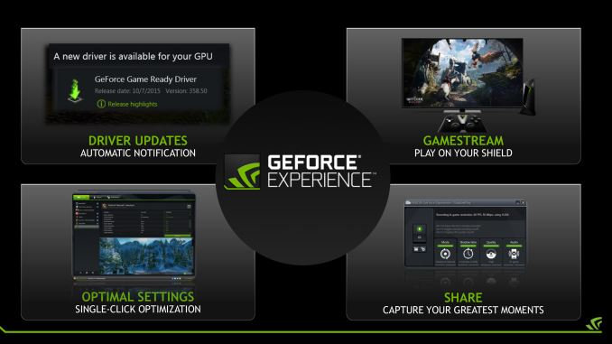
To kick things off, in a new beta release hitting NVIDIA’s servers today, NVIDIA will be updating several of GeForce Experience’s various NVENC-powered features to enable new features. On the GameStream front NVIDIA will be offering new functionality specifically targeted at the recently launched SHIELD Android TV set top box. With the SHIELD Android TV capable of decoding 4K video content, NVIDA is now giving GameStream the ability to encode video at that resolution, allowing for GameStream remote gaming at full native resolution for 4K TVs. Furthermore NVIDIA is also giving GameStream the ability to serve up 5.1 audio.

Until this latest release GeForce Experience had been limited to serving up GameStream with 1080p video and stereo audio, so this marks a significant increase in GameStream’s video and audio quality. At the same time because of the step up in quality the system requirements to use the new 4K mode are significantly higher as well. On the encode side only the newest Maxwell 2 generation GPUs have an NVENC unit capable of encoding at 4Kp60, so high-end Kepler users won’t see this functionality. Meanwhile on the reception side, a SHIELD Android TV is needed to receive 4K video, and NVIDIA is recommending a hardwired 100Mbps (or better) Ethernet connection for best performance. And on a technical side note, though not specified in NVIDIA’s presentation, as 4K support is limited to SHIELD Android TV I’m curious whether NVIDIA is still using H.264 or if they’re switched to HEVC, as Maxwell 2 and SHIELD Android TV support hardware HEVC encoding and decoding respectively.

Moving on, similar to GameStream, GeForce Experience’s video broadcasting module is also getting new functionality and an image quality boost. First launched with Twitch support back in late 2013, the broadcast module is now gaining support for Google’s rival YouTube Live service as well, allowing GeForce users to broadcast to the service of their choice. Furthermore the broadcast module can now upload video streams at 1080p60 with a maximum bitrate of 9Mbps, supplanting the module’s previous 720p60 limit. As even older versions of NVENC have long been able to record at 1080p, this change primarily appears to be NVIDIA increasing their limits now that these services are better able to handle the high bitrates that go with 1080p streaming.
The Next Few Months: Driver Updates Shift to GeForce Experience
Finally, in their last announcement for the day, NVIDIA is sharing a bit of information on their plans for GeForce experience for the rest of the year, and this is a big one.
Starting with a December update to GeForce Experience, NVIDIA will be overhauling how they distribute their driver updates. The company currently posts new drivers on a regular basis to their website while also simultaneously pushing them out via GeForce Experience. Come December, that will be changing and GeForce Experience will be the preferred “first access” distribution mechanism for NVIDIA’s frequent driver updates.
This change comes on the heels of NVIDIA’s latest research, which finds that 90% of all driver updates are now distributed through GeForce Experience. At this point NVIDIA is not discussing the change in great detail – and most likely they’re still sorting out the finer details of what they want to do – but the basic idea is to fully exploit the push update mechanism of GeForce Experience while drawing users into what will in time become a larger NVIDIA ecosystem. GeForce Experience will be used to distribute the company’s regular “point release” driver updates that the company frequently releases and typically contain bug fixes and performance improvements for gamers – in other words the drivers most gamers will want to be on. Meanwhile NVIDIA will still post drivers to their website (and by extension Windows Update), but on a reduced quarterly cadence.
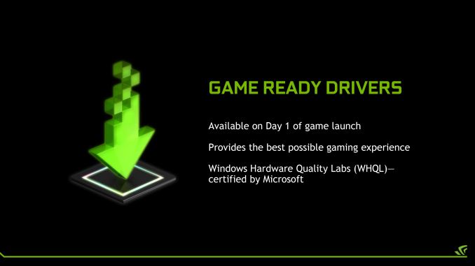
One thing NVIDIA has made clear is that they’re sticking with their overall Game Ready driver release system – targeting frequent driver updates to line up with major game launches – and this includes WHQL certification, so this won’t be NVIDIA cutting back on WHQL releases despite the fewer updates to their website. However even with WHQL certification, NVIDIA’s frequent driver releases (20 in just over the last year, not counting hotfixes) have been both a curse and a blessing for their wider user base, as non-gamers use the same drivers. I get the impression that this change is in part driven by a desire to establish separate “gamer” and “long term” driver release cadences where non-gamers aren’t constantly being bombarded by Game Ready point updates that primarily affect software they aren’t using.
At the same time however NVIDIA is also being straightforward about this driver change being part of a broader effort to promote GeForce Experience from a utility to a critical part of the GeForce ecosystem and to make it a software backend of sorts to their GPUs. The change in driver distribution will be accompanied by a yet to be fully detailed registration system where NVIDIA will be asking users to register their email addresses with GeForce Experience. NVIDIA has already been toying with this concept this year by using GeForce Experience to distribute game codes, so while it’s not fully clear what NVIDIA intends to do with a registered user base this is clearly the latest step as part of building their ecosystem.

More broadly speaking, NVIDIA has been pushing the larger GeForce ecosystem concept for even longer than GeForce Experience has been around – through G-Sync, PhysX, 3D Vision, and other technologies – and the company has made it clear for years that they see their continued success as coming from not just offering gamers solid hardware, but offering a wholly integrated experience. Given that PC gaming is otherwise one of the few bright spots in a tough market for PCs – year-over-year worldwide sales were down 7.7% for Q3 – it makes a great deal of sense for NVIDIA to want to further bolster their hand in the PC gaming market.
I am however curious to hear more details in the coming months about how the registration mechanism and revised driver distribution system works in GeForce Experience, what else NVIDIA will be doing with their growing ecosystem, and what GeForce owners think of this. Web based driver updates are older than the formal concept of the GPU, so NVIDIA’s plans mark a significant change in how drivers are at least preferably distributed. Though to NVIDIA’s credit they have clearly thought this through – even downgrading has been considered and NVIDIA will be building in a downgrade mechanism into the GeForce Experience driver update module. And ultimately with NVIDIA’s 90% distribution figure, it would appear that web downloads were already a quickly dying trend anyhow.
Wrapping things up, NVIDIA tells us these latest and upcoming improvements to GeForce Experience will be followed by further improvements for GeForce Experience in 2016. NVIDIA has stated that they have an “interesting roadmap” for the utility for the next year, one that will no doubt further flesh out this software ecosystem that the company is quickly assembling.
Read More ...
The Samsung Galaxy Tab S2 Review
The first Android tablet I ever used was the original Galaxy Tab. It was a 7" Android tablet running Android Froyo, and it seemed a lot like a large version of my Galaxy S. In hindsight, it wasn't a very good tablet, but Samsung was one of the first Android vendors to enter the market and they were working with a version of Android that had never been designed with tablets in mind. As Android moved to Gingerbread and then to the tablet exclusive release of Android Honeycomb, Samsung was always among the group of manufacturers producing Android tablets. While some vendors like LG and HTC have left and returned to the tablet market, Samsung has continually producing new Galaxy Tab tablets, and those tablets constitute a very large portion of the Android tablets that are sold each year. Read on for the AnandTech review of Samsung's newest tablet, the Galaxy Tab S2.
Read More ...
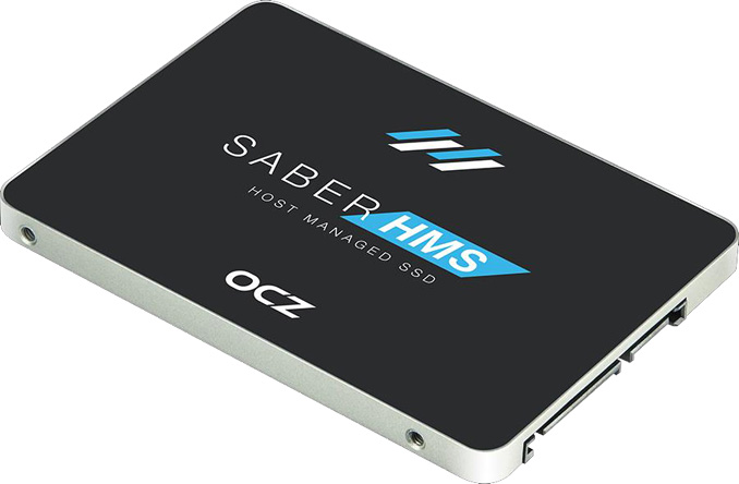
OCZ Announces First SATA Host Managed SSD: Saber 1000 HMS
Standardization efforts have been underway for more than a year in the committees for SAS, SATA, and NVMe, but OCZ's implementation is a pre-standard design that may not be compatible with what is eventually ratified. To provide some degree of forwards compatibility, OCZ is releasing an open-source abstraction library to provide what they hope will be a hardware-agnostic interface that can be used with future HMS devices.
OCZ's HMS implementation provides a vendor-specific extension of the ATA command set. A mode switch is required to access HMS features; when HMS mode is off the drive behaves like a normal non-HMS SATA drive and all background processing like garbage collection are managed autonomously by the SSD. When the HMS features are enabled, the host computer can request that the drive override normal operating procedure and disable all background processes, or to perform them as a high-priority task. If background processing is left disabled for too long, the drive will re-enable the background processing when needed and suffer the immediate performance penalty of the emergency garbage collection.
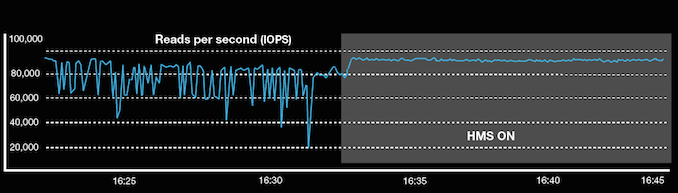
The intention is to allow better aggregate performance from an array of drives. An example OCZ gives is of an array divided into three pools of drives. At any given time, two pools are actively receiving writes, while the drives in the third pool are focusing solely on the "background" housekeeping operations. The two pools that are in active use defer all the background processing and operate with peak performance and consistency. By cycling the drive pools through the two modes, the intention is that none of the active drives will ever reach the steady-state of having constant background processing to free up space for the incoming writes. This provides a big improvement to performance consistency, and can also provide a minor improvement to overall throughput of the array.

Obviously, the load balancing and coordination required by such a scheme is not part of any traditional RAID setup. OCZ expects early adopters of HMS technology to make use of it from application layer code. HMS does not require any new operating system drivers, and OCZ will be providing tools and reference code to facilitate using HMS. They plan to eventually expand this to a comprehensive SDK, but for now everybody is in the position of having to explore how to best make use of HMS for their specific use case. For some customers, that may mean load balancing several pools of SSDs attached to a single server, while others may find it easier to temporarily offline an entire server for housekeeping.
OCZ has also envisioned that future HMS products may expand the controls from managing background processing to also changing overprovisioning or power limits on the fly, but they have no specific timeline for those features.
The drive OCZ is introducing with HMS technology is a variant of their existing Saber 1000 enterprise SATA SSD. The Saber 1000 HMS differs only in the SSD controller firmware; otherwise it is still a low-cost drive using the Barefoot 3 controller and is intended primarily for read-oriented workloads. Pricing is the same with or without HMS capability, though the Saber 1000 HMS is only offered in the 480GB and 960GB capacities. The warranty in either case is limited to 5 years, but because the HMS controls can affect write amplification, the Saber HMS write endurance rating is based on the actual Program/Erase cycle count of the drive rather than the total amount of data written to the drive.
| OCZ Saber 1000 HMS | ||
| Capacity | 480GB | 960GB |
| 4kB Random Read IOPS | 90k | 91k |
| 4kB Random Write IOPS | 22k | 16k |
| Random Read Latency | 135µs | 135µs |
| Random Write Latency | 55µs | 55µs |
| Sequential Read | 550 MB/s | 550 MB/s |
| Sequential Write | 475 MB/s | 445 MB.s |
| MSRP | $370 | $713 |
As a read-oriented drive with relatively little overprovisioning, the Saber 1000 has a lot to gain from HMS in terms of write performance and consistency, and it may allow the Saber 1000 HMS to compete in areas the Saber 1000 isn't fast enough for.
In addition to control over the garbage collection process, the Saber 1000 HMS provides a similar set of controls for managing when the controller saves metadata from its RAM to the flash. This is the information the controller uses to keep track of where each piece of data is physically stored and which blocks are free to accept new writes. Every write to the disk adds to the metadata log, so the changes need to be periodically evicted from RAM to flash. This is one of the key data structures that the drive's power loss protection needs to preserve, so the size of the in-RAM metadata log may also be limited by the drive's capacitor budget.
To enable software to make effective use of these controls, the Saber 1000 HMS provides an unprecedented view in to the inner workings of the drive. Software can query the drive for the NAND page size, erase block size, number of blocks per bank and number of banks in the drive. The total program and erase counts are reported separately, and information about free blocks is reported as the total across the drive as well as the average, maximum, and minimum per bank. The drive also provides a status summary of whether garbage collection or metadata log dumping are active, and whether they are needed. OCZ's reference guide provides recommendations for interpreting all of these indicators.
The Saber 1000 HMS will be available in early November for bulk purchases. The technical documentation and reference code should be available online today.
Read More ...
AMD Releases Catalyst 15.10 Beta Drivers
First off there are a few notes on Ashes of the Singularity. Along with providing performance and quality optimizations there is also a fixed issue with a 'Driver has stopped responding' error showing up while playing in DirectX 12 mode. AMD does note however that there still remains issues with the game crashing on some AMD 300 series GPUs and Ashes of the Singularity may fail to launch on some 2GB cards.
For Star Wars: Battlefront high performance graphics can now be used on devices running switchable graphics. AMD is also aware of a small number of users who are experiencing crashes with GTA V on some AMD Radeon R9 390X GPUs. Some changes have been made that should resolve the issue and they will continue to monitor user feedback on the problem.
On the stability front AMD has brought fixes for a couple of TDR errors which caused a crash when toggling between minimized and maximized mode while viewing 4K YouTube content or running the Unreal Engine 4 DirectX benchmark. Additionally playback issues with both MPEG2 and intermittent playback issues in Cyberlink PowerDVD when connected to a 3D display through HDMI have both been resolved. Lastly there was a problem with driver installation halting on some configurations that is now fixed.
Those interested in reading more or installing the drivers for AMD's desktop, mobile, and integrated GPUs can find them on AMD's Catalyst beta download page.
Read More ...
Consumer Reports Flexes Muscle, Hits Slumping Tesla Motors Stock
Tesla also has been struck with accusations of roughing up reporters at its gigafactor and by suggestions that the Model X is too pricey
Read More ...
Debunked: Beneath the Lies, Nigerian "Pee Generator" Is Still Pissing Into the Wind
Hydrogen doesn't grow on trees... well not free hydrogen gas, at least
Read More ...
Quick Note: Whoops, Microsoft Pushed Unwanted Windows 10 to Some Users
"Glitch" caused checkbox to default to enabled in Windows 7/8/8.1 causing some to be given an unexpected gift of Windows 10
Read More ...
CNN Resorts to Internet Censorship to Promote Clinton Over Senator Sanders
Meanwhile Sen. Paul continues to face similar attacks from the media, which is accused of favoring Trump
Read More ...
Available Tags:ASUS , HTC , Lenovo , Motherboards , ASRock , Xeon , Intel , AMD , NVIDIA , GeForce , Driver , Galaxy Tab , Samsung , Galaxy , OCZ , SATA , Catalyst , Microsoft , Windows ,
No comments:
Post a Comment