
AMD Announces Radeon R9 285, Shipping September 2nd
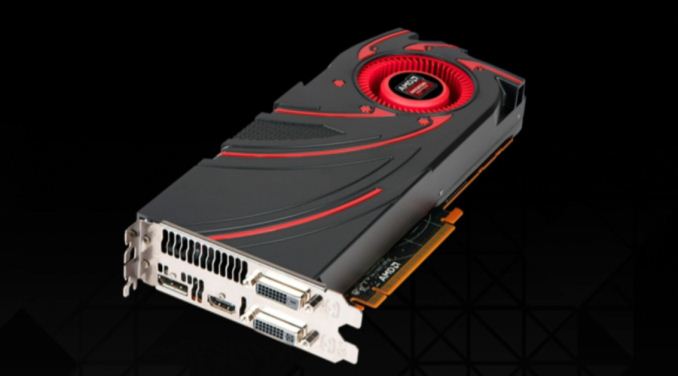
The R9 285 will take up an interesting position in AMD’s lineup, being something of a refresh of a refresh that spans all the way back to Tahiti (Radeon 7970). Spec wise it ends up being extremely close on paper to the R9 280 (née 7950B) and it’s telling that the R9 280 is no longer being advertised by AMD as a current member of their R9 lineup. However with a newer GPU under the hood the R9 285 stands to eclipse the 280 in features, and with sufficient efficiency gains we hope to see it eclipse 280 in performance too.
AMD GPU Specification Comparison |
||||||
AMD Radeon R9 290 |
AMD Radeon R9 280X |
AMD Radeon R9 285 |
AMD Radeon R9 280 |
|||
Stream Processors |
2560 |
2048 |
1792 |
1792 |
||
Texture Units |
160 |
128 |
112 |
112 |
||
ROPs |
64 |
32 |
32 |
32 |
||
Core Clock |
662MHz |
850MHz |
? |
827MHz |
||
Boost Clock |
947MHz |
1000MHz |
918MHz |
933MHz |
||
Memory Clock |
5GHz GDDR5 |
6GHz GDDR5 |
5.5GHz GDDR5 |
5GHz GDDR5 |
||
Memory Bus Width |
384-bit |
384-bit |
256-bit |
384-bit |
||
VRAM |
4GB |
3GB |
2GB |
3GB |
||
FP64 |
1/8 |
1/4 |
? |
1/4 |
||
TrueAudio |
Y |
N |
Y |
N |
||
Typical Board Power |
250W |
250W |
190W |
250W |
||
Manufacturing Process |
TSMC 28nm |
TSMC 28nm |
TSMC 28nm |
TSMC 28nm |
||
Architecture |
GCN 1.1 |
GCN 1.0 |
GCN 1.1? |
GCN 1.0 |
||
GPU |
Hawaii |
Tahiti |
Tonga? |
Tahiti |
||
Launch Date |
11/05/14 |
10/11/13 |
09/02/14 |
03/04/14 |
||
Launch Price |
$399 |
$299 |
$249 |
$279 |
||
Meanwhile feeding R9 285’s GPU falls to the card’s 2GB of GDDR5. This is on a 256-bit bus, and is clocked at 5.5GHz for a total memory bandwidth of 176GB/sec.
The R9 285 will have a rated typical board power (AMD’s analogue for TDP) of 190W. Notably this is only 10W higher than the Pitcairn based R9 270X despite the 40% larger SP count, or alternatively is 60W lower than the Tahiti based R9 280. While we don’t have a ton of details on the GPU at this time, taking into consideration the R9 270X comparison in particular, it’s clear that AMD has done some work on efficiency to squeeze out more compared to the GCN 1.0 based Pitcairn and Tahiti parts that R9 285 is going to be placed between.

Based on some prior AMD statements and information gleaned from AMD’s CodeXL tool, there is reason to suspect (but not confirm) that this is a newer generation design. AMD for their part has done something very similar in the past, launching GCN 1.1 back on the Radeon HD 7790, but essentially hiding access to and details of GCN 1.1’s feature set until the launch of the Hawaii based R9 290X later in the year. Whether AMD is doing this again remains to be seen, but it is something we have seen them do before and don’t doubt they could do again. Though whether they will confirm it is another matter, as the company does not like to publicly differentiate between GCN revisions, which is why even the GCN 1.1 name is unofficial.
Working for the moment off of the assumption that R9 285 is Tonga based and that it’s a GCN 1.1 part, we expect that performance should be a wash with the R9 280 while the R9 285 has an advantage on features. GCN 1.1 does have some mild performance optimizations to it that will give the R9 285 an edge, though it remains to be seen what the impact will be of the narrower memory bus. The fact that the Tahiti based R9 280X remains in AMD’s lineup indicates that if nothing else, it won’t match the performance of a full Tahiti configuration. Otherwise when it comes to features, being GCN 1.1 based means that the R9 285 will bring with it support for True Audio, support for bridgeless CrossFire thanks to the XDMA engine, GCN 1.1’s superior boost mechanism, and full support for AMD’s upcoming FreeSync implementation of DisplayPort Adaptive Sync (GCN 1.0 GPUs are not fully adaptive).

As for AMD, this offers the chance to refresh some of their oldest GCN 1.0 products with a more capable GPU while also cutting costs. While we don’t have die size numbers for Tonga, it is reasonable to expect that it is smaller due to the narrower memory bus along with the die size optimizations that we saw go into Hawaii last year, which means it will be cheaper to manufacture than Tahiti. This also brings down board costs, again due to the narrower memory bus and the lower TDP allows for simpler power delivery circuitry.

The R9 285 for its part will be launching at $249 on September 2nd. This will be a hard launch, and with AMD’s partners already posting product pages for their designs we suspect this will be a pure virtual (no reference card) launch. AMD also tells us that there will be both 2GB and 4GB cards; we’re going to have to see what the price premium is, as the suitability of 2GB enthusiast cards has been challenged by the presence of so much RAM on the current-generation consoles, which will have a knock-on effect on console-to-PC ports.
Though with the launch of the R9 285 and impending discontinuation of the R9 280, buyers looking at picking up an R9 285 in the near term will have to be on the looking for R9 280 on clearance sale. It’s already regularly found for $220 and lower, making it $30 cheaper than the R9 285 and possessing 3GB of VRAM to the R9 285’s 2GB. This will make the R9 280 a strong contender, at least until supplies run out.
Fall 2014 GPU Pricing Comparison |
|||||
AMD |
Price |
NVIDIA |
|||
Radeon R9 290 |
$400 |
||||
$310 |
GeForce GTX 770 |
||||
Radeon R9 280X |
$280 |
||||
Radeon R9 285 |
$250 |
||||
$240 |
GeForce GTX 760 |
||||
Radeon R9 280 |
$220 |
||||
Radeon R9 270X |
$180 |
||||
$160 |
GeForce GTX 660 |
||||
Both Alien Isolation and Star Citizen are still-in-development games. Alien Isolation is a first person shooter and is expected in October of this year. Meanwhile the space sim Star Citizen does not yet have a release date, and as best as we can tell won’t actually be finished until late 2015 at the earliest. In which case the inclusion here is more about access to the ongoing beta, which is the first time we’ve seen beta access used as part of a bundle in this fashion.

Read More ...
Habey Releases MITX-6771, J1900 Thin Mini-ITX with Long Life Cycle Support
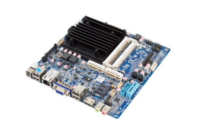

Habey MITX-6771 left, Intel DN2800MT right
Using
the 10W J1900 (quad core, 2.42 GHz) and a sufficient heatsink allows
Habey to continue its fanless range, but due to the thin mini-ITX
standard, motherboard design starts to get creative. The motherboard
supports two DDR3L SODIMM modules for up to 8 GB of DRAM, and storage
comes via an mSATA slot and a SATA 3 Gbps port. The mini-PCIe slot
supports SIM card adaptors (such as this one
suggested by Habey) to be used with the onboard SIM reader, with a
further PCIe 2.0 x1 slot for non-thin mini-ITX environments. Network
connectivity is either via the SIM card or the Realtek NIC.
The main aim for this sort of product is digital signage, industrial automation, medical, connected appliances and point-of-sale type systems, although Habey is keen to point out that media streaming is also a focus. Despite the limited one-year warranty, Habey is offering a Long Life Cycle Support package, although we are currently enquiring as to what this entails.
Users might note the lack of an ATX power connector on board, namely because power is either derived from the DC-IN jack on the rear IO or a 2-pin ATX connector just behind the DC-In. Inside the box is a SATA to two-pin ATX cable.

Source: Habey


Read More ...
Apple Begins iPhone 5 Battery Replacement Program for Certain Defective Devices
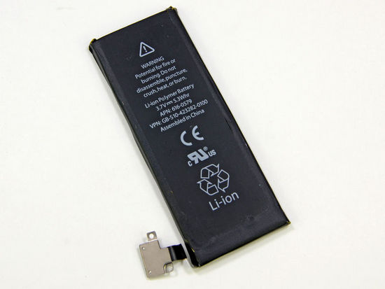
The replacement process for affected users will begin on August 22 in the United States and China, and on August 29 in the rest of the world. Apple recommends that users backup their iPhone to iTunes or iCloud and then wipe all user data prior to having their battery serviced. More information, as well as the service to check your device's serial number, can be found in the source link below.
Read More ...
AMD Celebrates 30 Years of Gaming and Graphics Innovation
AMD is apparently looking at a year-long celebration of the company formerly known as ATI, Radeon graphics, and gaming. While they're being a bit coy about the exact contents of the Livecast, we do know that there will be three game developers participating along with a live overclocking event. If we're lucky, maybe AMD even has a secret product announcement, but if so they haven't provided any details. And while we can now look forward to a year of celebrating AMD graphics and most likely a final end-of-the-year party come next August, why not start out with a brief look at where AMD/ATI started and where they are now?
 Source: Wikimedia Evan-Amos |
By 1987, ATI began moving into the world of PC graphics with their "Wonder" brand of chips and cards, starting with 8-bit PC/XT-based board supporting monochrome or 4-color CGA. Over the next several years ATI would move to EGA (640x350 and provided an astounding 16 colors) and VGA (16-bit ISA and 256 colors). If you wanted a state-of-the-art video card like the ATI VGA Wonder in 1988, you were looking at $500 for the 256K model or $700 for the 512K edition. But all of this is really old stuff; where things start to become interesting is in the early 90s with the launch and growing popularity of Windows 3.0.
 Source: Wikimedia Misterzeropage |
Two years later the Mach 32 came out, the first 32-bit capable chip with support for ISA, EISA, MCA, VLB, and PCI slots. Mach 32 shipped with either 1MB or 2MB DRAM/VRAM and added high-color (15-bit/16-bit) and later True Color (the 24-bit color that we're still mostly using today) to the mix, along with a 64-bit memory interface. And two years after came the Mach 64, which brought support for up to 8MB of DRAM, VRAM, or the new SGRAM. Later variants of the Mach 64 also started including 3D capabilities (and were rebranded as Rage, see below), and we're still not even in the "modern" era of graphics chips yet!
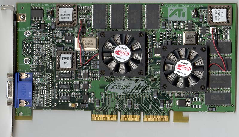 Rage Fury MAXX |
That part was followed by the Rage Pro, which is when graphics chips first started handling geometry processing (circa 1998 with DirectX 6.0 if you're keeping track), and you could get the Pro cards with up to 16MB of memory. There were also low-cost variations of the Rage Pro in the Rage LT, LT Pro, and XL models, and the Rage XL may hold the distinction of being one of the longest-used graphics chips in history, as I know even in 2005 or thereabouts there were many servers still shipping with that chip on the motherboard providing graphics output. In 1998 ATI released the Rage 128 with AGP 2X support (the enhanced Rage 128 Pro added AGP 4X support among other things a year later), and up to 32MB RAM. The Rage 128 Ultra even supported 64MB in its top configuration, but that wasn't the crowning achievement of the Rage series. No, the biggest achievement for Rage was with the Rage Fury MAXX, ATI's first GPU to support alternate frame rendering to provide up to twice the performance.
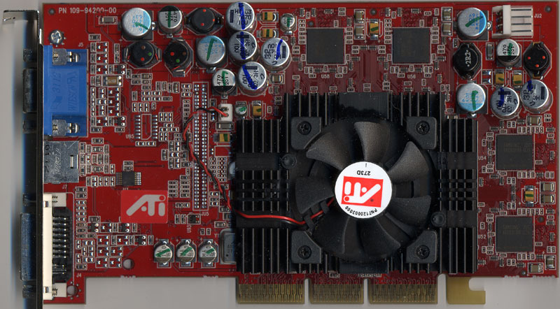 Radeon 9700 Pro |
Perhaps the best of the Radeon breed goes to the R300 line, with the Radeon 9600/9700/9800 series cards delivering DirectX 9.0 support and, more importantly, holding onto a clear performance lead over their chief competitor NVIDIA for nearly two solid years! It's a bit crazy to realize that we're now into our tenth (or eleventh, depending on how you want to count) generation of Radeon GPUs, and while the overall performance crown is often hotly debated, one thing is clear: games and graphics hardware wouldn't be where it is today without the input of AMD's graphics division!
That's a great way to finish things off, and tomorrow I suspect AMD will have much more to say on the subject of the changing landscape of computer graphics over the past 30 years. It's been a wild ride, and when I think back to the early days of computer games and then look at modern titles, it's pretty amazing. It's also interesting to note that people often complain about spending $200 or $300 on a reasonably high performance GPU, when the reality is that the top performing video cards have often cost several hundred dollars – I remember buying an early 1MB True Color card for $200 back in the day, and that was nowhere near the top of the line offering. The amount of compute performance we can now buy for under $500 is awesome, and I can only imagine what the advances of another 30 years will bring us. So, congratulations to AMD on 30 years of graphics innovation, and here's to 30 more years!

Read More ...
Lenovo Announces Trio Of Business PCs

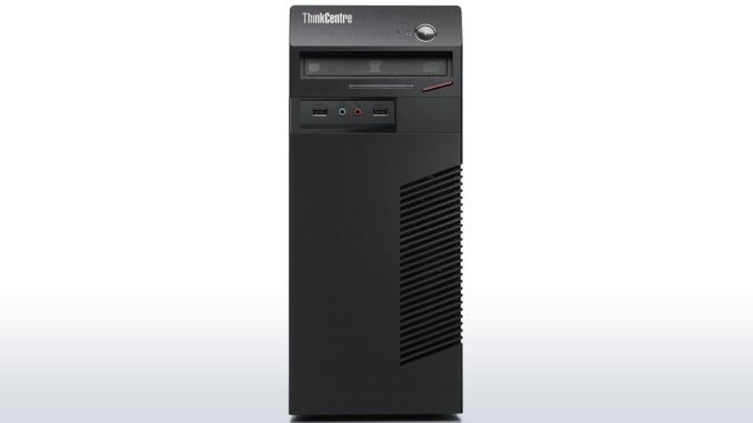 ThinkCentre M79 Mini Tower
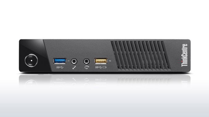 ThinkCentre M73 photo which shares the form factor with the M53
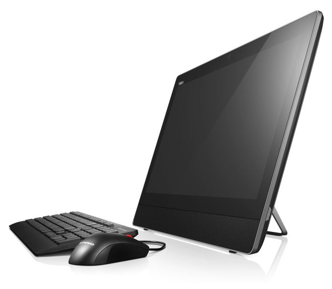 ThinkCentre E63z All-In-One
We do not have a full list of specifications for these devices at this time, but those should be available on the Lenovo site when they devices are made for sale.
Source:
Lenovo
Read More ...
G.Skill Announces Ripjaws DDR4, up to DDR4-3200
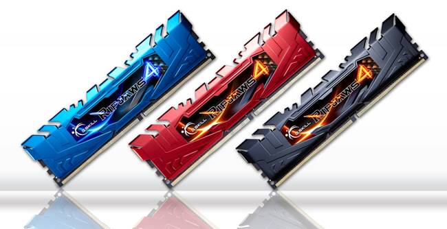
The new DDR4 from G.Skill is the next DRAM module manufacturer to come out with an official press release, and following the previous high performance Ripjaws DDR3 range G.Skill will introduce its memory under the Ripjaws 4 moniker with a new heatspreader design.


Preorder pricing puts these modules at:
DDR4-2133 C15 4x4GB: $260
DDR4-2400 C15 4x4GB: $280 / £240
DDR4-2666 C15 4x4GB: $300 / £290
DDR4-3000 C15 4x4GB: $400 / £380
DDR4-2133 C15 4x8GB: $480
DDR4-2400 C15 4x8GB: $530 / £440
DDR4-2666 C15 4x8GB: $550 / £500
Source: G.Skill


Read More ...
Measuring Toshiba's 15nm 128Gbit MLC NAND Die Size

Courtesy of Custom PC Review
At
Flash Memory Summit, Toshiba was showcasing their latest 15nm 128Gbit
MLC NAND wafer that has been developed in partnership with SanDisk. I
simply could not resist to calculate the die size as Toshiba/SanDisk has
not published it and die size is always the basis of any semiconductor
cost analysis. Unfortunately I was too busy running between meetings
that I did not take a photo of the wafer, so I am borrowing the picture
from Custom PC Review.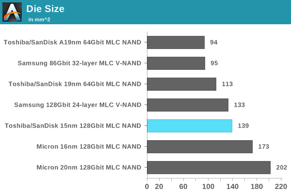
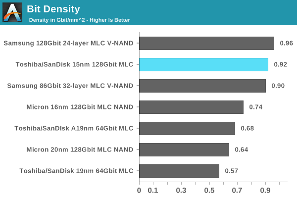
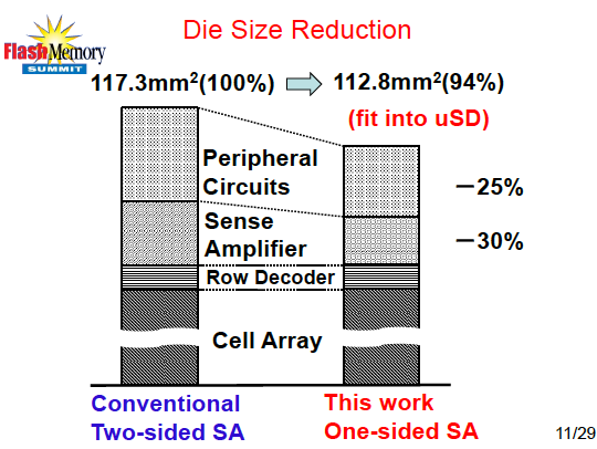
The production of Toshiba/SanDisk 15nm NAND node is currently ramping up and SSDs based on the new node are expected in Q4'14.
Read More ...
Interview with ADATA's President Shalley Chen
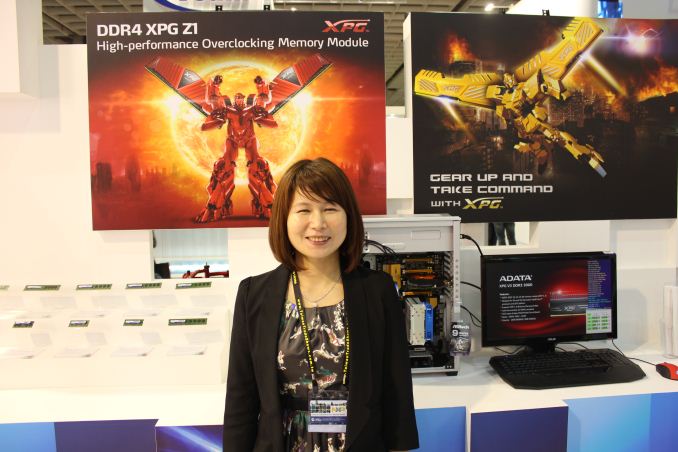
Before we get into the actual interview, I want to provide a brief overview of ADATA. The company generates over $1 billion in yearly revenue, which makes ADATA one of the largest memory companies in the world. Over a half of the revenue comes from the APAC (Asia-Pacific) region, which is logical given ADATA’s Taiwanese roots and the size of the Asian market. The North and Latin America region ranks as the second largest revenue source with about 15% share in total revenue, followed by Europe and other smaller regions. In the interview Mrs. Chen hinted that Asia, Europe and especially Russia are potential future growth areas for ADATA since the memory and SSD markets are still in a developing stage, whereas in the US the markets are more mature.
ADATA has had an office in the US since 2002 and employs 41 people across two offices in Los Angeles and Miami. These are both sales and customer support offices with the LA office in charge of North America while the Miami office is responsible for Latin America. All R&D is done in Taiwan at ADATA HQ whereas production is split between ADATA’s owned factories in China and Taiwan. While in Taiwan I took advantage of the offer to visit ADATA’s headquarters and the Taiwanese factory, as well as take some images for another article. Ever since the company was founded, ADATA has been a memory centric company. Like many companies of a similar nature, the mission, as it stood from day one, is to become the global leading brand of memory products. Although the product portfolio has grown over the years to include newer products such as USB flash drives, external hard drives, SSDs, memory cards, and, more recently, mobile power banks - fundamentally ADATA is still a memory company. Over half of ADATA’s revenue is generated by DRAM sales, and market researches rank ADATA as the Number Two DRAM module supplier in the world.
Given the high competition in the memory and SSD business, the question I always put to the manufacturers is this: what differentiates you from all the other brands? There are a dozen consumer focused DRAM companies, and there is little room for innovation or differentiation in the industry. Mrs. Chen told me that ADATA’s best weapon against the competition starts from the diversity of the product portfolio to the close relations with both chip suppliers and distributors. Mrs. Chen was keen to point out that ADATA makes products for all three major markets (client, enterprise and industrial), giving ADATA several different revenue sources, and the percentage of revenues from enterprise and industrial is getting bigger and bigger. This directly implies that the enterprise and industrial segments are substantial to ADATA.
Big enterprise OEMs like Intel and Samsung are typically interested only in large enterprises that buy upwards of tens of thousands of units, which leaves the small to medium size enterprise market to OEMs like ADATA to fight for the rest of the market. For example, some of Samsung’s enterprise products are only available to large OEMs (like EMC, Dell etc.), which leaves a niche for OEMs like ADATA and other smaller OEMs to offer better support for small to medium size enterprises. This also lends a benefit to work directly with the OEM for any customization.
Like other fabless DRAM and SSD manufacturers, ADATA does not manufacture the chips they use – ADATA have to buys them from the likes of Micron and Samsung. I asked if ADATA has ever thought about moving to chip fabrication, but the answer was negative. The main reason is the cost of a fab, and investing billions of dollars is a large risk. If we look at the major semiconductor fabricators, most of them have been in the industry for decades, developing new technologies as the research progresses. As a result, it would be extremely difficult for a new player to gain any significant market share without innovation or a wide product portfolio and mountains of investment (it is worth noting that innovation can come from start-ups that have new technology but get acquired). Another point ADATA raised is that it has close relations with DRAM and NAND suppliers, and thus has no need for a chip fab. In the end, the DRAM module industry is all about managing inventory against cost and potential sales, so the competitive advantage lies in forecasting the demand and managing the inventory efficiently.
The same applies to SSD controller development. Even though controllers can be fabricated by a third party, the capital required for the development and manufacturing is still a large sum. ADATA raised STEC as an example, which took the path to design its own controller platform but got into serious financial trouble due to the cost of the development. STEC ended up being acquired by Western Digital. ADATA does, however, have its own SSD firmware development team that has been in action since 2007. ADATA believes that the firmware team will play a key role to ensure competitiveness in the future. At this point in time, the team is mainly focusing on industrial SSD firmware development but there will be a change towards more unique firmware in the consumer side as well.
One of the big topics at Computex was the state of DDR4, and ADATA was heavily presenting its DDR4 portfolio at the show. Given ADATA’s position, the company wants to be the leader in DDR4 and will aim to push the new technology quite aggressively to both consumers and enterprises. ADATA is one of Intel’s six Haswell-E/X99 launch partners (the others are Micron, Samsung, Hynix, Kingston and Crucial), so there should be plenty of ADATA DDR4 available when the X99 platform launches later this year.
I asked ADATA whether the market for DDR4 will any different from current DDR3 from an OEM perspective. Mrs. Chen replied that DDR4 is different in the sense that right now DDR4 is mostly an enterprise product and will be sold through B2B marketing. The enterprise segment, due to the demand of more units per sale, also gets a greater benefit from DDR4, which is due to the lower voltage and higher frequency. The stereotypical scenario of hundreds of racks with each server equipped with eight to sixty-four DIMMs or more, lower power consumption on one module adds up and is thus always welcome. The speed should help enterprise workloads due to the tendency to be more often bound by memory performance than client workloads.
For the end-users, ADATA showed us there will be branded products at retail as well, but until the mainstream platform adopts DDR4, the enterprise segment will be the main market. In terms of production, ADATA believes that DDR4 will overtake DDR3 in H1’15 for the enterprise market, but the same will not happen in the consumer side until sometime in 2016.
All in all, there is a lot going on in both DRAM and SSD industries at the moment, so it will be interesting to see how the market reacts. We would like to thank Mrs. Chen and ADATA for their time giving us the opportunity to discuss the DRAM and SSD markets. As part of my visit to ADATA, I also met with ADATA’s DRAM and SSD directors to discuss their technology at a lower level. Keep your eyes peeled for that article in due course.
Read More ...
Recovering Data from a Failed Synology NAS
It was bound to happen. After 4+ years of running multiple NAS units 24x7, I finally ended up with a bricked NAS. Did I lose data? Were my recovery attempts successful? If so, what sort of hardware and software setup did I use? How can you prevent something like that from happening in your situation? Read on to find out.
Read More ...
SanDisk X300s (512GB) Review
Back in May SanDisk announced the X300s, which is the company's first SED (Self-Encrypting Drive). The X300s is based on the same Marvell platform as SanDisk's client drives but with the differentiation that the X300s is the only drive that supports encryption via TCG Opal and IEEE-1667 (eDrive) standards. Due to the encryption support the X300s is positioned as a business product since the main markets for encrypted drives are corporations and governments that handle sensitive and confidential data on a daily basis. SanDisk includes Wave's EMBASSY Security Center with every purchase of X300s, which allows Opal encryption on systems that are not eDrive compatible. Dive in to read more about the X300s, Wave's encryption software, and SEDs in general!
Read More ...
FMS 2014: Marvell Announces NVMe-Enabled PCIe 3.0 x4 88SS1093 SSD Controller
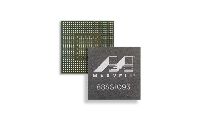
The 88SS1093 has support for 15nm MLC and TLC and 3D NAND, although I fully expect it to be compatible with Micron's and SK Hynix' 16nm NAND as well (i.e. 15nm TLC is just the smallest it can go). TLC support is enabled by the use of LDPC error-correction, which is part of Marvell's third generation NANDEdge technology. Capacities of up to 2TB are supported and the controller fits in both 2.5" and M.2 designs thanks to its small package size and thermal optimization (or should I say throttling).
The 88SS1093 is currently sampling to Marvell's key customers and product availability is in 2015. Given how well Intel's SSD DC P3700 fared in our tests, I am excited to see more NVMe designs popping up. Marvell has known to be the go-to controller source for many of the major SSD manufacturers (SanDisk and Micron/Crucial to name a couple), so the 88SS1093 will play an important part in bringing NVMe to the client market.
Read More ...
Examining Huawei's Benchmark Optimizations in the Ascend P7

Unfortunately, I have to talk about a case where this isn't true. While I've been working on reviewing the Ascend P7 and have found a lot to like, I am sure that the Ascend P7 alters CPU governor behavior in certain benchmarks. For those that are unfamiliar with the Huawei Ascend P7, it's considered to be Huawei's flagship smartphone. As Huawei's flagship, it's equipped with a Kirin 910T SoC, which has four Cortex A9r4 CPUs running at a maximum of 1.8 GHz, and two gigabytes of RAM. As a flagship smartphone, it also has a five inch display with a 1080p resolution.


Huawei Ascend P7 Performance |
|||||
Play Store |
Renamed |
Perf Increase |
|||
GFXBench T-Rex |
12.3 |
10.6 |
+16% |
||
3DMark Ice Storm U/L |
7462 |
5816 |
+28.3% |
||
In response to this issue, Huawei stated the following:
"CPU configuration is adjusted dynamically according to the workload in different scenarios. Benchmark running is a typical scenario which requires heavy workload, therefore main frequency of CPU will rise to its highest level and will remain so for a while. For P7, the highest frequency is 1.8GHz. It seldom requires CPU to work at the highest frequency for long in others scenarios. Even if the highest level appears, it will only last for a very short time (for example 400 ms). Situation is the same for most devices in the market."
Unfortunately, I'm not sure how this statement explains the situation, as two identical workloads performed differently. While I was hoping to see an end to rather silly games like this, it seems that this path before OEMs stop this kind of behavior will continue on for longer than I first expected. Ultimately, such games don't affect anyone that actually knows how to benchmark SoCs and evaluate performance, and one only needs to look to the PC industry to see that such efforts will ultimately be discovered and defeated.
Read More ...
MSI GS60 Ghost Pro 3K Review
MSI has several lines of gaming notebooks catering to different types of users. At the high-end is the GT series that supports the fastest mobile CPUs and GPUs while the GE series caters more towards the cost-conscious buyers. Somewhere in the middle is the GS line, which offers similar (or slightly higher) specifications to the GE series but delivers everything in a refined and more attractive chassis. Read on to find out how the GS60 with a 3K display compares to the other gaming laptops.
Read More ...
Unity Adds Native x86 Support for Android

As far as I can tell, none of the big game engines (Unity, Unreal Engine) were ported to x86 on Android. As a result, any game that leveraged these engines would be ARM code translated to run on x86. This morning Intel and Unity Technologies announced a native x86 version of the Unity game engine for Android. Selected developers have access to the x86 version today, and it'll be made available to everyone else by the end of the year. There's no charge for the update. Note that this only applies to the Android Unity port, the engine under Windows and all Windows tools are already obviously compiled for x86.
Intel's press release mentions support for both Core and Atom families. I clarified with Intel that the Core reference mainly applies to any Core M (Broadwell Y or Skylake Y) Android tablets, and not a push into Core based smartphones.
Intel is also working on enabling other game engines, but we'll have to wait to see those announcements.
Read More ...
FMS 2014: Silicon Motion Showcases SM2256 SSD Controller with TLC NAND Support
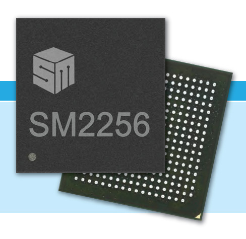
The SM2256 continues to be a 4-channel design and I am guessing it is also based on the same single-core ARC design with most changes being in the ECC engine. NAND support includes all NAND that is currently available including Toshiba's 15nm TLC NAND and the controller is designed to support 3D NAND as well. DDR3 and DDR3L are supported for cache and the controller is also TCG Opal 1.0 compliant.


The SM2256 is currently in customer evaluation and is expected to enter mass production in Q4'14 with shipping devices coming in late 2014 or early 2015.
Read More ...
SpaceX Falcon 9-R Rocket Suffers Malfunction, Self-Destructs During Test Flight
No injuries were reported following the mid-air explosion
Read More ...
Apple Starts Battery Replacement Program for “Very Small Percentage" of iPhone 5 Smartphones
Smartphones were sold between September 2012 and January 2013
Read More ...
No Free Play Day for You! Microsoft Says Apparent Promotion was an Error
Xbox Live Gold subscribers were excited about a potential new perk, but their celebration proved premature
Read More ...
BlackBerry Passport to Feature Snapdragon 800 Processor, 3,450 mAh Battery
BlackBerry's upcoming Passport actually has decent specs
Read More ...
From HULC to FORTIS: the Evolution of Lockheed Martin's Incredible Exosuit
New exoskeleton technology could increase worker productivity, cut injuries from aircraft and ship assembly
Read More ...
Moto X+1 Press Renders Leak, New Images Show Schematics for 4.7", 5.5" iPhone 6
@evleaks gives us one last "leak"
Read More ...
BlackBerry’s Latest "Plug" for its Passport Smartphone: Displaying Sharp X-rays for Doctors
BlackBerry says that the PassPort's 1440x1440 display is perfect for medical professionals
Read More ...
Sprint Introduces $60 Unlimited Plan, Touts $20/Month Costs Savings Versus T-Mobile
Sprint and T-Mobile are at it again
Read More ...
Opera Becomes Official Browser of Microsoft-Nokia's Non-Windows Phones
Licensing deal is a first for Opera's highly successful mobile effort
Read More ...
Microsoft Tests Free 24-Hour Xbox One Game Trials
Free game trials are a perk with Xbox One Gold subscription and mirror smartphone game sales tactics, PC history
Read More ...
Report: Microsoft to Announces Windows 9 on September 30
Microsoft is ready to move past Windows 8.x
Read More ...
HP Just Can’t Quit Windows 7; Offers Customers $170 Discounts on Windows 7 Laptops
According to Net Applications, Windows 8/8.1 market share is half that of Windows XP
Read More ...
Microsoft Wants Windows 8.1 Inside Children's Toys, Appliances
"Internet of Things" 174 MB build of Windows 8.1 can now run on Intel Quark SoC: we're guessing Metro isn't included
Read More ...
New Photos Show “Assembled” iPhone 6, Protruding Camera Ring
Apple iPhone 6 will launch on September 9
Read More ...
Leaked Qualcomm Roadmap: 20 nm 64-bit Octacore Smartphone SoCs Cometh
New chip stacking tech and a 20 nm process will accompany Qualcomm's Snapdragon 205, 410, 610, 615, 805, 808, and 810
Read More ...
ZTE Nubia 5S mini LTE 4.7" Smartphone Headed to U.S. for $280 Unlocked
The Nubia 5S mini LTE is a well-rounded device, but disappoints on battery life and camera quality
Read More ...
Available Tags:AMD , Radeon , iPhone 5 , Apple , iPhone , Gaming , Lenovo , SSD , MSI , Android , Motion , iPhone 5 , Microsoft , BlackBerry , iPhone 6 , Sharp , Windows Phone , Opera , Xbox , Windows , Windows 7 , HP , Windows , Windows , Windows 8 , Windows , iPhone 6 , Smartphone , ZTE , Smartphone ,
No comments:
Post a Comment