
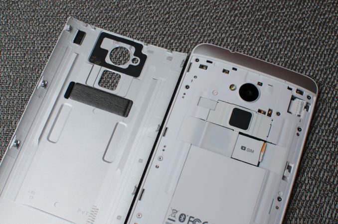
A Post about Removable Storage, Removable Batteries and Smartphones
Let's get through the basics first:
All else being equal, removable storage and user replaceable batteries aren't inherently bad things. In fact, they can offer major benefits to end users.
The key phrase however is "all else being equal". This is where the tradeoff comes in. On the battery front, the tradeoff is very similar to what we saw happen in notebooks. The move away from removable batteries allows for better use of internal volume, which in turn increases the size of battery you can include at the same device size. There are potential build quality benefits here as well since the manufacturer doesn't need to deal with building a solid feeling removable door/back of some sort. That's not to say that unibody designs inherently feel better, it's just that they can be. The tradeoff for removable vs. integrated battery is one of battery capacity/battery life on a single charge. Would you rather have a longer lasting battery or a shorter one with the ability the swap out batteries? The bulk of the market seems to prefer the former, which is what we saw in notebooks as well (hence the transition away from removable batteries in notebooks). This isn't to say that some users don't prefer having a removable battery and are fine carrying multiple batteries, it's just that the trend has been away from that and a big part of the trend is set based on usage models observed by the manufacturers. Note that we also don't penalize manufacturers for choosing one way or another in our reviews.
The tradeoffs are simple with an internal battery, the OEM doesn't need to include a rigid support structure on the battery to prevent bending, and doesn't need to replicate complicated battery protection circuitry, and can play with alternative 3D structures (so called stacked batteries) for the battery and mainboard as well. Personally, I'd rather have something that lasts longer on a single charge and makes better use of internal volume as that offers the best form factor/battery life tradeoff (not to mention that I'm unlikely to carry a stack of charged batteries with me). It took a while for this to sink in, but Brian's recommendation to charge opportunistically finally clicked with me. I used to delay charging my smartphone battery until it dropped below a certain level and I absolutely needed to, but plugging in opportunistically is a change I've made lately that really makes a lot of sense to me now.
The argument against removable storage is a similar one. There's the question of where to put the microSD card slot, and if you stick it behind a removable door you do run into the same potential tradeoff vs. build quality and usable volume for things like an integrated battery. I suspect this is why it's so common to see microSD card slots used on devices that also have removable batteries - once you make the tradeoff, it makes sense to exploit it as much as possible.

There's more to discuss when it comes to microSD storage however. First there's the OS integration discussion. Google's official stance on this appears to be that multiple storage volumes that are user managed is confusing to the end user. It's important to note that this is an argument targeted at improving mainstream usage. Here Google (like Apple), is trying to avoid the whole C-drive vs. D-drive confusion that exists within the traditional PC market. In fact, if you pay attention, a lot of the decisions driving these new mobile platforms are motivated by a desire to correct "mistakes" or remove painpoints from the traditional PC user experience. There are of course software workarounds to combining multiple types of storage into a single volume, but you only have to look at the issues with SSD caching on the PC to see what doing so across performance boundaries can do to things. Apple and Google have all officially settled on a single storage device exposed as a single pool of storage, so anything above and beyond that requires 3rd party OEM intervention.
The physical impact as well as the lack of sanctioned OS support are what will keep microSD out of a lot of flagship devices.
In the Android space, OEMs use microSD card slots as a way to differentiate - which is one of the things that makes Android so popular globally, the ability to target across usage models. The NAND inside your smarpthone/tablet and in your microSD card is built similarly, however internal NAND should be higher endurance/more reliable as any unexpected failures here will cause a device RMA, whereas microSD card failure is a much smaller exchange. The key word here is should, as I'm sure there are tradeoffs/cost optimizations made on this front as well.
The performance discussion also can't be ignored. Remember that a single NAND die isn't particularly fast, it's the parallel access of multiple NAND die that gives us good performance. Here you're just going to be space limited in a microSD card. Internal NAND should also be better optimized for random IO performance (that should word again), although we've definitely seen a broad spectrum of implementation in Android smartphones (thankfully it is getting better). The best SoC vendors will actually integrate proper SSD/NAND controllers into their SoCs, which can provide a huge performance/endurance advantage over any external controller. Remember the early days of SSDs on the PC? The controllers that get stuffed into microSD cards, USB sticks, etc... are going to be even worse. If you're relying on microSD cards for storage, try to keep accesses to large block sequentials. Avoid filling the drive with small files and you should be ok.
I fully accept that large file, slow access storage can work on microSD cards. Things like movies or music that are streamed at a constant, and relatively low datarate are about the only things you'll want to stick on these devices (again presuming you have good backups elsewhere).
I feel like a lot of the demand for microSD support stems from the fact that internal storage capacity was viewed as a way to cost optimize the platform as well as drive margins up on upgrades. Until recently, IO performance measurement wasn't much of a thing in mobile. You'd see complaints about display, but OEMs are always looking for areas to save cost - if users aren't going to complain about the quality/size/speed of internal storage, why not sacrifice a bit there and placate by including a microSD card slot? Unfortunately the problem with that solution is the OEM is off the hook for providing the best internal storage option, and you end up with a device that just has mediocre storage across the board.
What we really need to see here are 32/64/128GB configurations, with a rational increase in price between steps. Remember high-end MLC NAND pricing is down below $0.80/GB, even if you assume a healthy margin for the OEM we're talking about ~$50 per 32GB upgrade for high-speed, high-endurance internal NAND. Sacrifice on margin a bit and the pricing can easily be $25 - $35 per 32GB upgrade.
Ultimately this is where the position comes from. MicroSD cards themselves represent a performance/endurance tradeoff, there is potentially a physical tradeoff (nerfing a unibody design, and once you go down that path you can also lose internal volume for battery use) and without Google's support we'll never see them used in flagship Nexus devices. There's nothing inherently wrong with the use of microSD as an external storage option, but by and large that ship has sailed. Manufacturers tend to make design decisions around what they believe will sell, and for many the requirement for removable storage just isn't high up on the list. Similar to our position on removable batteries, devices aren't penalized in our reviews for having/not-having a removable microSD card slot.
Once you start looking at it through the lens of a manufacturer trying to balance build quality, internal volume optimization and the need for external storage, it becomes a simpler decision to ditch the slot. Particularly on mobile devices where some sort of a cloud connection is implied, leveraging the network for mass storage makes sense. This brings up a separate discussion about mobile network operators and usage based billing, but the solution there is operator revolution.
I'm personally more interested in seeing the price of internal storage decrease, and the performance increase. We stand to gain a lot more from advocating that manufacturers move to higher capacities at lower price points and to start taking random IO performance more seriously.
     |
Read More ...
Thecus N2560: Intel's EvanSport NAS Platform Review
NAS units targeting home consumers have traditionally been underpowered in terms of hardware as well as firmware features. Low power, reduced cost and media-centric features are primary requirements in this area. Despite being loath to participate in this market segment, Intel decided to jump into the fray due to the explosive growth potential. The EvanSport Atom-based SoC platform was launched in March 2013 to cater to this market segment. Better known as Berryville (its tag in the set-top-box arena), this SoC integrates two Atom cores (based on the Bonnell microarchitecture) along with a bunch of media-centric features as well as I/Os to make it suitable for the NAS market. Read on to find out how the Thecus N2560 (one of the first EvanSport-based NAS units to hit the market) fares in our evaluation.
| |
Read More ...
Best Desktop CPUs: Holiday 2013

So obviously there are many facets to a processor choice: price, performance, affinity to software, low power, gaming (single GPU and SLI/Crossfire) and single core performance all play a role. A lot of our recommendations here are based on behind the scenes testing as well as reviews we have done over the past 12-24 months, including:
- 10/3/2013: Choosing a Gaming CPU, October 2013
- 9/7: Analyzing the Price of Mobility: Desktops vs. Laptops
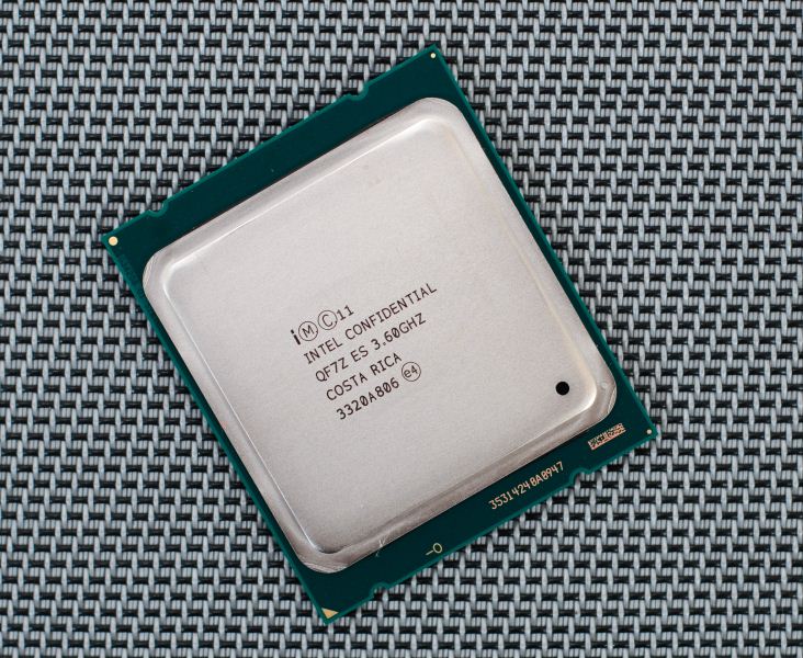
- 9/3: Intel Core i7 4960X (Ivy Bridge E) Review
- 6/6: AMD's Richland vs. Intel's Haswell GPU on the Desktop: Radeon HD 8670D vs. Intel HD 4600
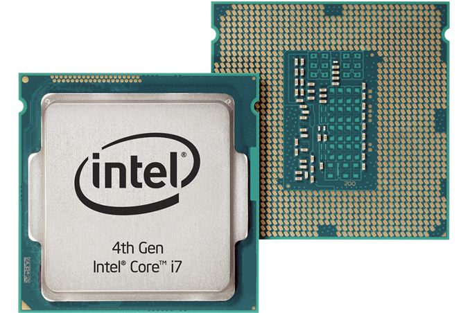
- 6/1: The Haswell Review: Intel Core i7-4770K & i5-4670K Tested
- 5/23: The AMD Kabini Review: A4-5000 APU Tested
- 1/15: Dragging Core2Duo into 2013: Time for an Upgrade?
- 10/23/2012: The Vishera Review: AMD FX-8350, FX-8320, FX-6300 and FX-4300 Tested
- 10/2: AMD A10-5800K & A8-5600K Review: Trinity on the Desktop
Extreme Performance, Need Threads: Intel i7-4930K on X79 ($580, 6C/12T at 3.4 GHz)
Despite any zeitgeist against the extreme platforms, there are a lot of users that can justify the cost, purely because it improves their work flow, or they want to say they have an extreme system, whether or not it is always used. For users who need to stick to consumer level hardware (i.e. not Xeons, because of price) then the obvious choice for almost all workloads is the Intel i7-4930K processor. The other main contenders here are the i7-4960X ($1050, 3.5 GHz), i7-4820K (4C/8T, $330, 3.7 GHz) and the i7-4771 (4C/8T, $320, 3.5 GHz) on Z87. We plunge for the 4930K due to it being the cheaper of the twelve threaded processors, as well as offering some headroom for overclocking should users require that facility. Using an Ivy Bridge-E processor also opens up to a 64 GB of memory, although the downside is that the X79 platform is looking a little old against 990FX and Z87, and extra SATA 6 Gbps/USB 3.0/Thunderbolt connectivity is still under the guise of newer platforms. Nevertheless, building a system of this grunt today puts the 4930K in the firing line given Haswell-E is a good number of months (12+?) away.
For users that do not want to invest into the X79 platform at such a high price point, the obvious answer is to look at the i7-4771 on H87 (for non-overclocking) or i7-4770K on Z87 with a small bump in frequencies.
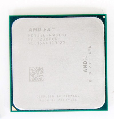
AMD Throughput: AMD FX-8320 on 990FX ($160, 4M/8T at 3.5 GHz)
The debate about pure performance of Intel vs. AMD is almost clear cut depending on what type of operations you want to perform. AMD’s architecture for Bulldozer and Piledriver mean that it acts somewhere between a quad and an octo-core, depending on if you are using floating point operations (fractions) or integer (whole number, pure hexadecimal) operations in code respectively. AMD went with this architecture because operating system logic is mostly the latter, which offers up more multithreading opportunities. Unfortunately due to the lack of IPC (somewhat negated by clock speed) and that the real world is not too kind, the quad module offerings from AMD only perform better than their Intel counterparts in specific scenarios or applications. Certain video editing and synthetic benchmarks (Cinebench) love the AMD architecture, which doubles up in benefit when considering the price. In this circumstance, the FX CPU we suggest is the FX-8320. The other CPUs worth considering are the FX-8350 ($200, 4.0 GHz), the FX-9370 ($290, 4.4 GHz) and the FX-8300 (3.3 GHz), and there is recourse to look at the FX-8350 for $40 more and +500 MHz off the bat, but the FX-8320 gets the nod if AMD is your weapon of choice in this arena.
Looking back at our Gaming CPU recommendations and results (where we test CPUs at stock), the CPU we suggest is the i5-4670K. Our testing shows that this CPU, with 2/3/4 graphics cards, offers top or near top performance compared to other CPUs – the multithreaded advantage of the 4770K or 4960X was only observable at the extremely high end, and even then the differences were not that great. Certain games take more of a hit than others, and for the vast majority of titles today the focus lies on good core performance for when these games start properly using as many threads as necessary (it is harder to program than you think).
For overclocking, as always your results will vary. For example, I have played with three i7-4770K CPUs. Two of them were not bad, getting 4.6 GHz and 4.7 GHz at 1.300 volts respectively. The third one is absolute trash, hitting its maximum at 4.2 GHz with 1.400 volts. The 4670K is almost a third less than the 4770K, meaning if you are wanting a high enough overclock, it is less of a hit you sell on the CPU to buy another. For extreme overclockers, the 4670K also provides an alternative for the older benchmarks while using sub-zero cooling.
Gaming Single CPU:
- Intel i3-4330 on H87 ($160, 2C/4T @ 3.6G) or
- AMD Athlon II X4 760K on FM2+ / A88X ($90, 2M/4T @ 3.8G) or
- AMD Athlon II X4 651K on FM1 / A75 (£61, 4C/4T, 3.0G)
Choosing a CPU for gaming on a single GPU is a little tougher than a multi-GPU test. At this end of the spectrum (where most gamers are), it all becomes rather title dependent. Some games are designed to use as many cores as you can throw at it (Battlefield), whereas others will perform the same no matter what is in the system (Sleeping Dogs). As a result, I have picked a few worth mentioning that might be on offer this season.
The first up is one of the new Intel Haswell dual cores with hyperthreading. Up until the dual core CPUs were released, my recommendation was a quad core i5-4340 ($190, 4C/4T, 3 GHz) which we tested in our Gaming CPU article. But given my comments above, and the since introduction of the dual core Haswells, the i3-4330 is a pretty exciting choice. It offers the potential for more performance (4 threads at 3.6 GHz), comes in slightly cheaper, and will have a better single thread throughput. The only downside will be that there are not four real cores, but game engine designers have been working with Hyperthreading as the main form of extra threading for a few generations now. I have recommended the H87 chipset here (or B85), due to the focus on no-overclocking and single GPU that might help save a few pennies in the overall build.
For something a little cheaper, the AMD Athlon II X4 760K might be worth a look. This is the CPU version of the equivalent Richland APU, meaning no integrated graphics: but if we are talking a single discrete GPU, then integrated graphics is not that relevant here. As the 760K is based on Richland, this means two modules with up to four threads of integer computation. Game development is slowly getting the idea that if possible, make calculations integers rather than floating point, but we are still a bit away in that department: the 3.8 GHz and $90 price tag help the 760K be a suitable choice up until that point. I have suggested going for an FM2+ motherboard here, because in January the new Kaveri APUs (and non-APU equivalents) should be released, meaning that an upgrade is only a processor away.
My final recommendation is actually a bit of an old one, and most likely not available new everywhere, but still possible to find on various websites. The AMD Athlon II X4 651K is a Llano CPU, which dates back to before AMD made the change to Bulldozer based modules. This means that the 651K is a full-bodied quad core, rather than a dual module/quad thread hybrid. At 3.0 GHz and lower IPC than Intel, it still has some room to grow with a little overclocking, but in games that do require a full and proper quad core to get going, then the 651K is an opportunity. One downside perhaps is using the FM1 socket and A75 chipset, although it is not too dissimilar to the newer A88X chipset on FM2+.
Gaming on Integrated or Hybrid graphics: AMD A10-6800K on FM2+ ($140, 2M/4T at 4.1 GHz)
There are market segments that rely on integrated graphics for gaming, and at this juncture there is only one real integrated GPU we can recommend: the A10-6800K with its 384 SPs at 844 MHz and recommended memory of 2133 MHz as well. While you get the best integrated graphics performance currently available on a desktop CPU, there are two things worth noting: the APU itself has a TDP of 100W, and Kaveri is just around the corner. The first point could be negated by using the A10-6700 APU, which has the same integrated graphics for only 65W but is slightly slower (3.7 GHz) and a bit more expensive ($149). The point about Kaveri coming dates back to AMD’s announcement for release on January 14th, where it was announced that the top end Kaveri APU will feature 512 SPs (similar to a HD 7750) at 720 MHz, with a CPU speed of 3.7 GHz and a rated 856 GFLOPS. If you need an integrated graphics solution for gaming today, we recommend picking up an FM2+ motherboard so Kaveri can drop straight in.
General Day-to-Day, Low Power:
- Intel Pentium G3430 on H81 ($100, 2C/2T at 3.3GHz Haswell)
- AMD did announce two 45W models (6500T and 6700T, neither of which are at retail yet)
Day to day performance is often very subjective. What feels lightning fast for some may feel sluggish to others, and it is not always the CPU that is the culprit – I recommend everyone upgrading to SSDs as boot drives for operating system builds, however I have met with system builders who have clients that insist that only one drive letter is present on their new office systems (insert SSD caching). When it comes down to a daily CPU, there are plenty that cover the bases for word processing, light photo editing, checking eBay and email: in fact most of these are covered by tablets, and the low end desktop market is shrinking as a result. Nevertheless, I built my family a small home system recently, and at the time having something that would feel quick was important. Low power is another factor, which swings us around to the low powered ‘T’ processors from both Intel and AMD.
But there are caveats: Newegg and Amazon seem to avoid the ‘T’ processors, at least when it comes to Haswell. The consumer markets (from what I can tell) focus more on the ‘S’ variants, which are not particularly low power. My recommendation falls at the Pentium G3320T for Intel, a 35W 2.6 GHz Haswell dual core part, which should be sufficient for most families when paired with an SSD, but this does not seem to exist outside OEMs. At this point, our other options include the G3430, which Newegg does stock, although it does pull 54W. For AMD, it was announced that two low powered models would be coming to market (the A8-6500T and A10-6700T) on September 18th, however I have yet to see either at retail, perhaps suggesting that these are only available in the US to OEMs for now.
Low Power, High Throughput:
- i7-4765T on H87 (£256, 4C/8T @ 2G) or
- i7-4770T on H87
One review sample that has come in recently is the ASRock M8 barebones – a mini-ITX chassis with PSU and a Z87 motherboard. The motherboard uses a 4+1 power delivery, albeit without a heatsink and requiring airflow over the VRMs – so while the motherboard supports overclocking, I cannot be 100% confident I want something very warm in a small space, but I still want it to be powerful.
After looking at processors for the best part of a couple of weeks, my best result was actually a Xeon, one of the models that is binned for high frequency and low voltage, thus making the power consumption low. This was the E3-1230L V3, a 25W quad core CPU with hyperthreading running at 1.8 GHz and turbo to 2.8 GHz. This theoretically would produce an i5-4670K like performance at full multithreaded load at less than 1/3 of the power usage. Alas, this CPU is truly for servers only, and not even eBay through up many results. Speaking with Intel UK, they suggested a similar CPU in the i7-4765T.
The i7-4765T is almost the Xeon equivalent, being a 35W quad core CPU with hyperthreading, but running at 2.0 GHz with turbo up to 3.0 GHz. For the power consumption, this CPU seems to fly, even in gaming. The only downside of the CPU is the lack of availability: I seem to find it for sale easily enough in the UK (for the same price as a 4770K), but not in the US in any immediate timeframe.
The fall back processor is the standard i7-4770T, which moves the TDP to 45W, still a quad core with hyperthreading, but running at 2.5 GHz and turbo up to 3.7 GHz. However our dilemma of finding locations where the ‘T’ processors are sold rears its head again, with any location offering them having a ‘1-3 week’ lead time.
Another position to take would be to look at a normal CPU and downclock it to reach the desired power envelope. Almost all CPUs will allow you to reduce the multiplier and the voltages down (-K or non-K SKU), but it requires a level of manual tinkering not unlike overclocking to reach the desired level. The benefit of the ‘T’ SKUs is obviously they will work out of the box like it says they should.
To Conclude:
There never is a killer CPU that covers all avenues. Even if Intel or AMD (or Via) offer a CPU that performs better than anything with low power and a massive integrated GPU installed, it is not going to come cheap. Each of our suggested price brackets has their contenders nearby, especially when comparing Intel to AMD as to a preferred build or total price. One of AnandTech’s biggest suggestions over time is to invest in an SSD if you have not already (SSD buyer’s guide incoming), then if you are a gamer to focus on the GPU, and then analyze which CPU/motherboard you really need for your system. Picking the right one helps in the long term, and perhaps saves a few $ for an upgrade in another area. Hopefully the holiday sales are kind this year!
| |
Read More ...
Enermax Case, Heatsink/Fan and Power Supply Giveaway: Holiday 2013
Going into this holiday season we're fortunate enough to have wonderful sponsors eager to show their support for AnandTech readers by providing us with some hardware to give away. First on the list is Enermax. If you're in need of a new case, CPU cooler and power supply you're going to want to enter this one.
| |
Read More ...
Western Digital Releases Black^2: 120GB SSD + 1TB HD Dual-Drive in 2.5" Form Factor

WD Black2 combines a 120GB SSD and a 1TB 5400rpm hard drive into one 2.5" 9.5mm solution. WD doesn't actually call the Black2 a hybrid drive, but a dual-drive because the the SSD and hard drive are completely separate. In other words, the drive will appear as two separate volumes: 120GB SSD and 1TB hard drive. There's no caching involved and the end-user can decide what goes to the SSD as if it were a standalone drive. By default only the SSD portion is usable but WD supplies a USB drive with drivers in the retail package to make the hard drive portion visible to the OS as well. All Windows versions from XP and up are supported but there is no OS X support at the time of launch.
| WD Black2 Specifications | |
| Interface | SATA 6Gbps |
| Sequential Read | 350MB/s |
| Sequential Write | 140MB/s |
| Power Consumption | 0.9W (idle/standby) / 1.9W (read/write) |
| Noise | 20dBA (idle) / 21dBA (seek) |
| Warranty | 5 years |
| MSRP | $299 |
Update: Techreport has already received their sample and opened it up, which revealed JMicron's JMF667H controller. We don't have any prior experience with the controller but generally JMicron's controllers have not been the greatest but it's been years since we've tested a JMicron based drive so things might have changed.
Update 2: WD initally told us that the drive is a single-platter design but they've now corrected their earlier statement. The hard drive consists of two 500GB platters as some of you suspected in the comments.
Given that most laptops only have room for one 2.5" drive by default, I do see a potential market for the Black2. In the past consumers have had to make the choice between a fast but small SSD or a large but slow hard drive. The Black2 eliminates the need to do that compromise. However, I'm disappointed for the lack of caching support. WD told us that they conducted market studies and according to those end-users wanted full control of the SSD and data. I don't completely agree because the reason why most consumers have negative thoughts about caching is because the available cache sizes are just way too small. Apple is the only one who has done it right with Fusion Drive by not going any smaller than 128GB, while others are trying to get by with 8-32GB. The Black2 has enough NAND for a pleasant caching experience, so not including caching software is a letdown. Technically you could use third party caching software but I still would have hoped for a solution from WD, preferably something user-configurable so it's not forced like in the Momentus XT.
| |
Read More ...
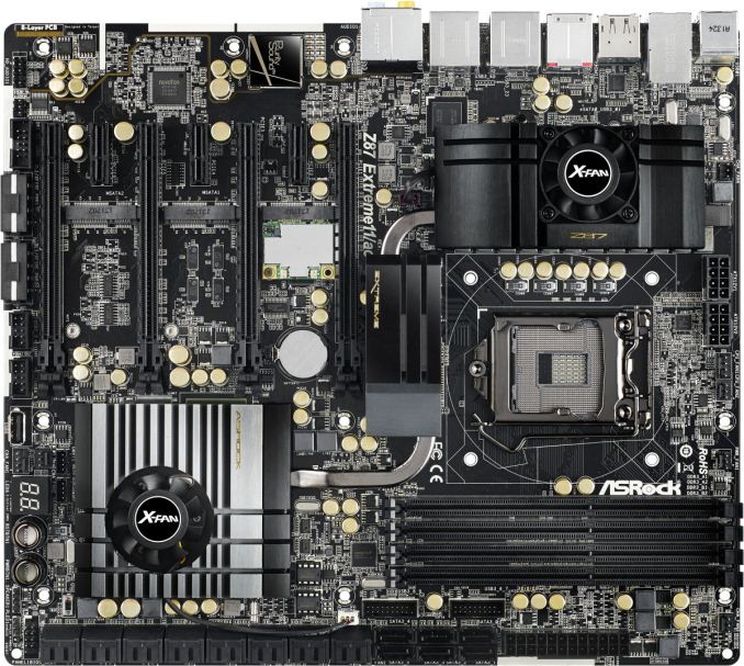
ASRock Launch Z87 Extreme11/AC with 22 SATA Ports and the H81 Pro BTC for Cryptocurrency Mining


At the time, we postulated on the PCIe lane allocation, as ASRock had said that this was possible with only one PLX 8747 switch, whereas on the Z77 Extreme11 they had used two. It all comes down to the LSI 3008, which requires eight PCIe lanes by itself. Since that iteration, ASRock have also added Thunderbolt 2 into the mix, using a controller that requires 4 PCIe lanes to give two TB2 ports. This also goes along with four-way SLI and Crossfire, suggesting that using switches they are able to supply x8/x8/x8/x8 to the GPUs, another x8 to the LSI chip and x4 to the TB2 controller. Without getting the board on hand, I would assume that the motherboard disables part of the PCIe slots in order to use Thunderbolt 2.

The other board coming out of ASRock is somewhat aptly timed. Bitcoin and Cryptocurrencies have been up and down in the news this past year, and even today Bitcoin has hit $660 with Litecoin going above $8.50. Back around the Bitcoin blowout earlier this year, I pitched around the idea of a motherboard built with cryptocurrency mining in mind. ASRock responded in kind, with the H81 Pro BTC and H61 Pro BTC:


As always, despite what ASRock PR might have you believe, I would like to add a disclaimer: there is no guarantee that Bitcoin mining (via ASIC or GPU) will generate a financial return. Only invest what you can afford to lose.
Nevertheless, I would hope that these motherboards would be sold in the $60 or below segment. That seems awfully low for a motherboard, but therein defines the purpose of such a product in the cryptocurrency world. The US Senate is expected to report on Virtual Currency today, which could explain the recent influx of investment into Bitcoin and Litecoin.
| |
Read More ...
Patriot Viper III Review: 2x4 GB at DDR3-2400 C10-12-12 1.65 V
Perhaps I am out of the loop, but in recent CPU generations of PC building, Patriot Memory has not featured much on my radar. A quick look at their product range tells a tale: the fastest DDR3 kits are 2400 MHz, and by comparison to some other memory manufacturers, their presence at Computex was somewhat discreet. Nevertheless, when I got in contact for our series of quick fire Haswell memory reviews, Patriot were keen to sample a couple of their 2x4 GB Viper III kits of DDR3-2400 C10 1.65V.
| |
Read More ...
Netgear Launches ReadyNAS 716 6-bay 10-GbE Desktop NAS
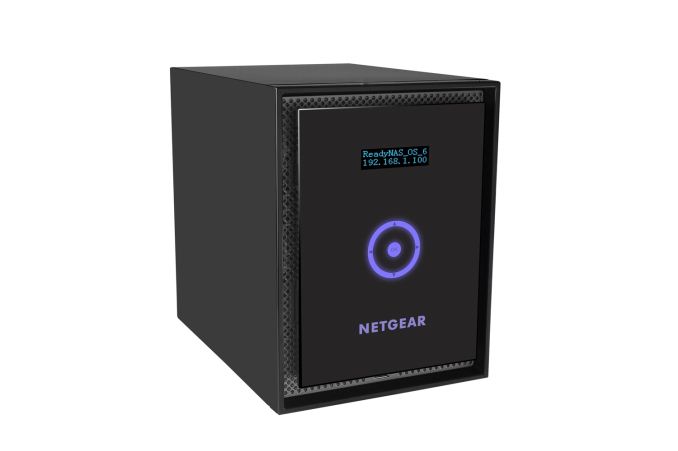
10 GbE capabilities have been restricted to rackmount units so far, but we are seeing vendors slowly recognize the scope for those capabilities in the desktop / tower form-factor. QNAP launched its TS-x70 series last month and touted its 10 GbE-readiness. By default, those units come with dual GbE cards in the expansion slot making for a total of four GbE ports in each unit. Netgear is going one step further with the RN716 by bundling a dual 10 GbE card in the expansion slot along with the two GbE ports already on the motherboard.
The ReadyNAS RN716 is based on an Intel Xeon x86 platform and comes with ECC DRAM making it a full-fledge server solution for business and enterprise users. The following table presents the detailed specifications of the RN716x.
| Netgear ReadyNAS 716 Specifications | |
| Processor | Intel Xeon E3-1265L V2 (4C/8T, 2.5 GHz) |
| RAM | 16 GB ECC DDR3 RAM |
| Drive Bays | 6x 3.5"/2.5" SATA 6 Gbps HDD / SSD (Hot-swappable) |
| Network Links | 2x 1 GbE + 2x 10 GbE |
| USB Slots | 2x USB 3.0 / 3x USB 2.0 |
| eSATA Slots | 3x (compatible with EDA500 expansion chassis) |
| Expansion Slots | 1x (occupied by 2x 10 GbE card, not user-replaceable) |
| VGA / Display Out | HDMI |

| |
Read More ...
IBM and NVIDIA Announce Data Analytics & Supercomputer Partnership
First and foremost, on the software side of matters IBM and NVIDIA are announcing that the two are collaborating on adding GPU acceleration to IBM’s various enterprise software packages, most notably IBM’s data analytic packages (InfoSphere, etc). Though generally not categorized as a supercomputer scale project, data analytics can be at times a significantly compute bound task, making it a potential growth market for NVIDIA’s Tesla business.

Of course IBM is very much a vertically integrated company, offering mixes of software, hardware, and services to their customers. So any announcement of GPU acceleration for IBM’s software would go hand in hand with a hardware announcement, and that’s what’s occurring today.
So along with IBM and NVIDIA’s software collaboration, the two are announcing that IBM will begin building Tesla equipped Power computers in 2014. IBM announced POWER8 back at Hot Chips 2013, and along with a suite of architectural improvements to the processor itself, it’s the first Power chip to be specifically designed for use with external processors via its CAPI port, and as such it’s the first POWER chip well suited for being used alongside a Tesla card.
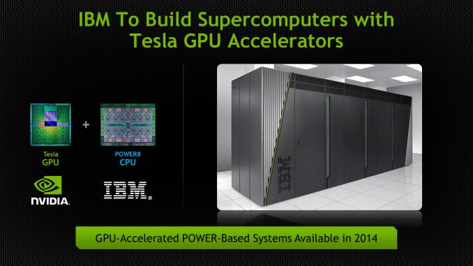
On a final note, it’s worth pointing out that all of this comes only a few months after IBM formed the OpenPOWER Consortium, of which NVIDIA is also a member. For the moment we’re just seeing the barest levels of integration between NVIDIA’s GPUs and IBM’s POWER CPUs, but a successful collaboration between the two would leave the door open to closer works between the two in the future. Both companies offer licensing of their respective core IP, so if NVIDIA and IBM wanted to make a run at the server/compute market with a fully integrated APU, this would be the first step towards accomplishing that.
| |
Read More ...
LSI Announces SandForce SF3700: SATA and PCIe in One Silicon
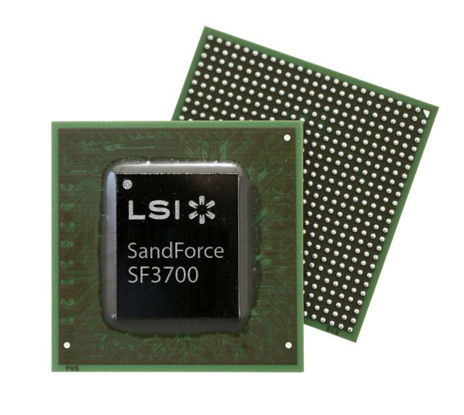

Now that SandForce is under the LSI umbrella, its designs seem a little more forward looking. The SF3700 is a more modular design than its predecessors. The front end, core and back end of the SoC are all modular. Adding support for new types of NVM (e.g. 3D NAND) should be far easier, not to mention the flexibility in adapting to new interface standards. Given that we're in a transition period between SATA and PCIe, modularity on the front end will come in handy as we start looking at interfaces beyond PCIe gen 2.
On the back end interface side, the SF3700 has nine NAND channels (I'll get to that soon) that are compatible with both Toggle-Mode and ONFI NAND. SandForce has always supported a variety of different NAND configurations and this is the case with SF3700 too. You can pretty much use any NAND (including TLC) that is currently in the market and as outlined above SandForce can and will quickly adapt to NAND changes in the future. Similar to earlier SandForce controllers, the SF3700 doesn't use any extrernal DRAM either -- the NAND mapping table and other crucial bits of data are stored in the controller's internal SRAM.
It's impossible to ship a modern SSD controller without talking about PCIe these days. Thankfully, the SF3700 supports both SATA 6Gbps and PCIe 2.0 x4. That's a single silicon offering with support for both interfaces. The interface is selectable during manufacturing at the drive level. End users won't be able to switch between interfaces, but drive makers can quickly shift production between SATA and PCIe drives all with the same silicon.

| The SF3700 Family | ||||
| SKU | SF3719 | SF3729 | SF3739 | SF3759 |
| Market | Entry Client | Mainstream Client |
Enthusiast Client
Value Enterprise
|
Enterprise Caching
Enterprise Storage
|
| Interface | SATA + PCIe x2 | SATA + PCIe x2 | PCIe x4 | Scalable PCIe |
| Suggested Form Factors | M.2 | M.2 | M.2 & 2.5" | HHHL |

The SF3700 is still a few months away from retail availability, but LSI did provide us with some performance targets for its reference drive based on the controller (256GB/512GB).
| LSI SandForce SF3700 Expected Performance (Worst Case) | ||
| Interface | PCIe 2.0 x4 | SATA 6Gbps |
| Random Read | 150K IOPS | 94K IOPS |
| Random Write | 81K IOPS | 46K IOPS |
| Sequential Read | 1800MB/s | 550MB/s |
| Sequential Write | 1800MB/s | 502MB/s |
LSI's targets are far from humble as it's shooting for 1.8GB/s for the PCIe 2.0 x4 version, which is only 200MB/s short of the theoretical 2GB/s limit. LSI is expecting to be able to hit these performance targets, but it's not quite there yet. Based on LSI's own tests, they've been able to achieve 1.45GB/s sequential read speed with early firmware. Power consumption specs have not been finalized either but LSI said that currently the power consumption is about 4W, which they are trying to bring down by optimizing the firmware. Idle power consumption should be even lower than SF-2200's and support for low idle power technologies such as DevSleep are present.

IO consistency and low latency operation are both priorities for the SF3700. The SF-2000 family was one of the more consistent set of performers from the previous generation, it's good to see LSI prioritizing this going forward though.
Improved DuraWrite
DuraWrite is what made SandForce's previous controllers unique. DuraWrite is SF's proprietary technology that minimizes NAND writes by reducing writes on the fly through real-time compression and/or data de-duplication. The SF3700 comes with improved DuraWrite and LSI is claiming noticeably better data reduction capability. In other words, the SF3700 should be able to compress low entropy data even more and feature lower write amplification as a result, which in turn results in higher endurance and also better performance at small capacities with less NAND die. High entropy data won't see huge improvements in performance based on the algorithm alone.

SF's RAISE (Redundant Array of Independent Silicon Elements) technology also gets updated with the SF3700. The original RAISE only protected against a single page or block failure but the SF3700 offers a second level RAISE for more protection. With the second level RAISE enabled, the drive can withstand a failure of multiple pages and blocks or up to a full die. The downside of course is that the new RAISE also needs more capacity for redundancy, which in this case is two die. In case of a die failure, the drive can either allocate another die by reducing the over-provisioning or it can switch back to first level RAISE (i.e. the original RAISE).
The new RAISE also solves the mystery of the ninth NAND channel. OEMs can use the ninth channel to overcome the capacity reduction that RAISE causes. OEMs no longer have to decide between higher capacity and RAISE as they can use the ninth channel for RAISE and still have eight left for actual user data (in reality the RAISE workload is equally distributed across all nine channels). SandForce OEMs can build a drive with for example 288GiB of NAND, which can then be sold as a 256GB drive with default over-provisioning and RAISE enabled (in this case, second level RAISE would take 32GiB and the 7% over-provisioning would come from the Gibibyte to Gigabyte translation). Obviously the redundancy data is not physically located in the ninth NAND package as it's spread across all the die.

The final new feature of RAISE is Fractional RAISE. The problem with the original RAISE was that using a full die for redundancy wasn't efficient. For example in a 64GiB SSD that would have been 1/8 (8GiB) of all the capacity and the usable capacity would have ended up being around 56GB, which isn't very attractive from a marketing perspective. Fractional RAISE is designed for small capacities with low die-count and it uses less than a full die, so OEMs can use RAISE without having to reduce the usable capacity to an odd number. Of course Fractional RAISE will not protect against a full die failure but it's still better than what small SSDs had before (i.e. nothing).
SHIELD
The final new feature of the SF3700 controller is SHIELD, LSI's updated error correction engine. One side effect of moving to lower process geometries with NAND is an increase in the number of errors you encounter when trying to read from or program to a device. The error rate also increases over the life of the NAND. The reality is that the ECC algorithm you'll need at the beginning of your drive's life is going to be different than what you need near the end. Shield works by cycling through a number of different ECC algorithms to find the optimum balance between performance and reliability. Early on when accesses come back error free, Shield defaults to very low latency ECC. If the error rate starts to climb, Shield will switch to other more sophisticated forms of ECC - trading off latency for reliability.

The same tradeoff can apply to the amount of area you use to store ECC data. SF3700 offers the option for drives to vary the percentage of each NAND page reserved for ECC data on the fly. This can theoretically give you more capacity early on in the life of your drive, and more endurance as your NAND ages. Obviously you'll need OS support in order to have a drive with variable capacity, so don't expect this to apply to most consumer platforms today.

SandForce expects the combination of Shield and adaptive code rate will allow drives to go from ~3K program/erase cycles to 18K cycles with 10nm class NAND.
Final Thoughts and Availability
There is a ton of potential in SF3700. If LSI is able to get the performance to the expected level, the SF3700 will likely be the fastest consumer-orientated PCIe solution we've seen. LSI's main goal with the SF3700 was to design a controller that takes the current and upcoming challenges of NAND into account. As we move to smaller lithography NAND, features like DuraWrite and RAISE become even more important because NAND endurance, reliability and performance get lower.
I truly hope that LSI/SandFoce has learned from the mistakes of SF-2200 and they'll validate the product enough before releasing it to the public. The SandForce brand image took a huge hit thanks to issues associated with SF-2200 (not to mention the outright denial of aforementioned issues for months). A repeat of that with the SF3700 is out of the question if this brand is to survive. I do expect the situation to be very different this time around, which is likely part of the reason why we're hearing about drives in the market in the first half of 2014 - 3.5 years after the introduction of the SF-2000 family of controllers. The SF3700 will be built under LSI's supervision and with LSI's resources as well, both of which should hopefully make for a better outcome than previous SF designs.

There is still a lot of work to do since the firmware is still in an early stage and to be honest, I wouldn't be surprised if we don't see drives in retail until closer to the middle of next year. As long as the end result is a stable, well validated product, I'm fine with that.
| |
Read More ...
NVIDIA Launches Tesla K40

With both the GeForce and Quadro lineups getting the full GK110 treatment in the last couple of months with GeForce GTX 780 Ti and Quadro K6000 respectively, it was only a matter of time until NVIDIA gave the Tesla lineup the same treatment. Tesla K20(X) was of course the first product to launch with NVIDIA’s flagship GK110 GPU, and now with K40 the Tesla lineup will become the final product line to be upgraded to full GK110 specifcations.
| NVIDIA Tesla Family Specification Comparison | ||||||
| Tesla K40 | Tesla K20X | Tesla K20 | Tesla M2090 | |||
| Stream Processors | 2880 | 2688 | 2496 | 512 | ||
| Core Clock | 745MHz | 732MHz | 706MHz | 650MHz | ||
| Boost Clock(s) | 810MHz, 875MHz | N/A | N/A | N/A | ||
| Shader Clock | N/A | N/A | N/A | 1300MHz | ||
| Memory Clock | 6GHz GDDR5 | 5.2GHz GDDR5 | 5.2GHz GDDR5 | 3.7GHz GDDR5 | ||
| Memory Bus Width | 384-bit | 384-bit | 320-bit | 384-bit | ||
| VRAM | 12GB | 6GB | 5GB | 6GB | ||
| Single Precision | 4.29 TFLOPS | 3.95 TFLOPS | 3.52 TFLOPS | 1.33 TFLOPS | ||
| Double Precision | 1.43 TFLOPS (1/3) | 1.31 TFLOPS (1/3) | 1.17 TFLOPS (1/3) | 655 GFLOPS (1/2) | ||
| Transistor Count | 7.1B | 7.1B | 7.1B | 3B | ||
| TDP | 235W | 235W | 225W | 250W | ||
| Cooling | Active/Passive | Passive | Active/Passive | N/A | ||
| Manufacturing Process | TSMC 28nm | TSMC 28nm | TSMC 28nm | TSMC 40nm | ||
| Architecture | Kepler | Kepler | Kepler | Fermi | ||
| Launch Price | $5499? | ~$3799 | ~$3299 | N/A | ||
Perhaps more significantly however, with K40 the Tesla family finally gets access to 4Gbit GDDR5 modules, which have only recently reached mass production. With Tesla K20X previously topping out at 6GB (24 x 2Gbit), NVIDIA is taking K40 to 12GB (24 x 4Gbit), making it the first Tesla card with that much memory. Like Quadro K6000, which is also launching with 12GB of VRAM, NVIDIA has a number of customers in the compute market who are bottlenecked at either the algorithmic or data set levels by memory capacity. So the additional capacity should offer a welcome improvement for those users, and unlock at least a few more workloads that couldn’t properly fit inside of 6GB.

But with that said, despite the fact that K40 is just an iteration on K20 and a member of the Kepler Tesla family (as opposed to being a new product line of its own), K40 does come with one new trick that the K20 cards did not: GPU Boost. To be clear here this isn’t the same GPU Boost we saw in NVIDIA’s Kepler GeForce cards – for one thing it’s not automatic – but it is similar. Since these cards are both TDP limited and all of the cards in a cluster need to operate at the same clockspeed to maintain synchronization, NVIDIA cannot ship K40 at a higher clockspeed than it’s going to be able to sustain. However that doesn’t mean the GK110 GPU underlying K40 can’t clock higher (we’ve seen it in GTX 780 Ti) so NVIDIA has split the difference and will be offering selectable clockspeeds under the GPU Boost moniker.

On a further note, there is one last feature upgrade that is new for K40. For K20(X) NVIDIA limited those cards to PCI Express 2.0 speeds, despite the fact that the underlying hardware was designed to support PCI Express 3.0. For K40 however NVIDIA is finally enabling full PCI Express 3.0 speeds, which would coincide the launch of Intel’s Ivy Bridge-E hardware and the fixed compatibility between the two platforms. For the relevant systems this offers to double the available bandwidth between individual Tesla cards and between cards and the host CPUs – going from 8GB/sec to 15.75GB/sec – something that relative to the high-speed local memory was at times a massive bottleneck for these cards.

| |
Read More ...
Xbox? PCs? Mobile? Microsoft Wants One Windows to Rule Them All
From the smartphone to the game console, Microsoft thinks it can make one size fit all
| |
Read More ...
Intel Works With Google and Microsoft to Add 64-Bit Support for Bay Trail Tablets
Bump will allow for faster graphics, cryptography and high-def video processing, future-prep tablets
| |
Read More ...
Quick Note: Windows 8.1 Touchscreen Ultrabooks Hit Firesale Prices on Amazon
E-tailer slashes up to a third off poorly selling ultrabook models
| |
Read More ...
BlackBerry Says Goodbye to CFO, COO, CMO
To top it off, BlackBerry board member Roger Martin has resigned
| |
Read More ...
Mayor Bloomberg Says No More Styrofoam Dishes in NYC, Says it Can Cause Cancer
Ban could affect a variety of businesses ranging from homeless shelters to fast food joints
| |
Read More ...
Facebook CEO Says Government "Blew It" with NSA Spying
Although he feels bad for the government in terms of the HealthCare.gov issues
| |
Read More ...
Japan Gives Top U.S. Politicians a Free Ride, Sales Pitch on New Maglev Trains
Central Tokyo Railways is willing to license for U.S. use, but future in America remains uncertain
| |
Read More ...
WD Shows Off New SSD, HDD Dual Drive
It's the first to hold both drives separately in one laptop drive (and it's not a hybrid)
| |
Read More ...
Apple Acquires Kinect Sensor Maker PrimeSense
Apple purchased it for around $360 million USD
| |
Read More ...
5.25" Samsung Galaxy Grand 2 Smartphone Gets Official
Pricing and availability for the new phablet remains a mystery
| |
Read More ...
Ford is Ready for Aggressive Rollout of Fuel Saving Start-Stop Technology
No word on when the aggressive roll out will begin
| |
Read More ...
11/25/2013 Daily Hardware Reviews -- Western Digital Black² Dual Drive Edition
DailyTech's roundup of reviews from around the web for Monday
| |
Read More ...
11/24/2013 Daily Hardware Reviews
DailyTech's roundup of reviews from around the web for Sunday
| |
Read More ...
Available Tags:Western Digital , SSD , ASRock , SATA , IBM , NVIDIA , Microsoft , Windows , Intel , Google , Windows 8 , Amazon , BlackBerry , Facebook , CEO , HDD , Apple , Kinect , Samsung , Galaxy , Smartphone , Ford , Western Digital , Hardware , Hardware ,
No comments:
Post a Comment