
ARM Cortex A12: Between Cortex A9 and A15 in Power & Perf, Sampling in Late 2014


The
comparison point here is the Cortex A15 and Cortex A7, but the latter
should be quite performance competitive with a Cortex A9 so the
comparison is still relevant. The Cortex A15 island in Samsung’s Exynos 5
Octa occupies 5x the die area as the A7 island, and consumes nearly 6x
the power. In exchange for 5x the area and 6x the performance, the
Cortex A15 offers under 4x the performance. It’s not exactly an area or
power efficient solution, but a great option for anyone looking to push
the performance envelope.
Today, ARM is addressing that hole with the Cortex A12.
This
announcement isn’t a deep architectural disclosure, but we do have some
high level details to share. Like AMD’s Jaguar, Intel’s Silvermont and
even ARM’s A9, the Cortex A12 is a dual-issue out-of-order architecture.
Unlike the Cortex A9, the Cortex A12 is fully out-of-order including
the NEON/FP units (NEON/FP was in-order on Cortex A9).
Pipeline
length increased a bit compared to Cortex A9 (11 stages), however ARM
told me to expect similar frequencies to what we have with the Cortex
A9.
The
execution back end has also been improved, although I don’t have many
details as to how. My guess is we should expect something a bit wider
than Cortex A9 but not nearly as wide as Cortex A15.
Memory
performance is much improved compared to Cortex A9 as well, which we’ve
already demonstrated as a significant weak point in the A9
architecture.
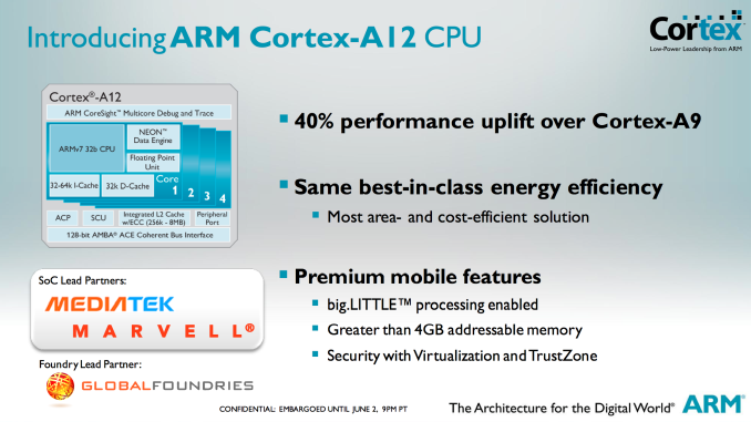
All
of the architectural enhancements are supposed to provide up to a 40%
increase in performance (IPC) over Cortex A9 at the same frequency and
process node. ARM isn’t talking power, other than to say that it can do
the same workload at the same power as a Cortex A9. In order words,
Cortex A12 should have higher power than Cortex A9 but faster execution
reduces total energy consumed. With a higher max power we’ll see more
dynamic range in power consumption, but just not nearly as much as with
the Cortex A15.
Cortex
A12 also adds support for 40-bit memory addressability, an intermediate
solution before we get to 64-bit ARMv8 based architectures. Finally,
Cortex A12 features the same ACE bus interface as Cortex A7/A15 and can
thus be used in big.LITTLE configurations with either core (but likely
exclusively with the A7s). Given the lower power profile of Cortex A12,
I'm not sure the complexity of doing a big.LITTLE implementation will be
worth it though.


ARM
expects the Cortex A12 to be used in mainstream smartphones and tablets
where cost and power consumption are a bit more important. The design
makes a lot of sense, the only downside is its launch timeframe. ARM
expects to be sampling Cortex A12 in late 2014 with the first devices
showing up in 2015. Update: ARM clarified that SoCs based on
Cortex A12 would be shipping to device vendors in mid-2014, with devices
shipping to consumers by late 2014 to early 2015. ARM has optimized
Cortex A12 processor packs at both Global Foundries (28nm SLP) and TSMC
(28nm HPM).

Read More ...
ARM Mali-T622 & V500 Video Block Complement Cortex A12

The Mali-T622 is a 2-core implementation of the 2nd generation Mali-T600 GPU architecture that we first learned about with the 8-core T628. Each shader core features two ALUs, an LSU and a texture unit.

On the video front, the Mali-V500 video encode/decode block is a multi-core engine used for all video acceleration. The V500 allegedly supports up to 100Mbps High Profile H.264, although details are scarce on more specifics. ARM claims support for up to 120 fps 4K video decode with an 8-core V500 implementation. Mali-V500 also features a protected video path, necessary for gaining content owner support for high-bitrate/high-resolution video decode.

The V500 also supports ARM's Frame Buffer Compression (AFBC), a lossless compression algorithm that can supposedly reduce memory bandwidth traffic by up to 50%. There's presently no frame buffer compression in Mali GPUs today, but ARM expects to eventually roll AFBC out to Mali GPUs as well.


Read More ...
Gigabyte Launching Two New Haswell Xeon Server Motherboards
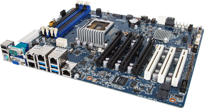
First up is the GA-6LXSV, a tower and rack capable ATX motherboard featuring Intel’s C224 chipset, support for up to 32GB of ECC/nonECC, and quad Intel gigabit Ethernet (I210).
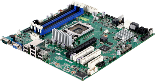
Next up is a motherboard clearly named by a northern British designer, being called the GA-LASS. This is a micro-ATX motherboard for compact systems, again listed as both for rack and tower. By contrast to the GA-6LXSV, the connectivity is significantly reduced – a single Intel NIC, two SATA 6 Gbps, four SATA 3 Gbps and a single PCIe 3.0 x16.
Specific launch dates and pricing are as yet unannounced. Typically Gigabyte server boards do not enter general sale, but with enough interest we might see some cropping up on official e-tailers. System integrators should get in contact with their local Gigabyte server sales team for information.
Over recent months we have had a look at a couple of Gigabyte’s motherboard server range, and I am speaking to their Server guys this week while in Computex. Is there any particular model anyone would like to see reviewed at AnandTech?
Read More ...
Intel's Haswell - An HTPC Perspective: Media Playback, 4K and QuickSync Evaluated
Over the last two years, the launch of every major desktop CPU family from both AMD and Intel has been accompanied by a dedicated HTPC-oriented article. This coverage has been complementary to Anand's extensive analysis from a general computing perspective. Haswell will be no different.
The advancements made from Llano to Trinity and from Sandy Bridge to Ivy Bridge had rendered entry level platforms good enough for casual / mainstream HTPC users. Advanced users still require discrete GPUs for using some video renderers and obtaining accurate display refresh rates. Each vendor has their own quirks when it comes to driver features and stability. This has made it difficult to declare any one solution as the perfect HTPC platform. Intel has hyped up improved GPU performance in the lead up to Haswell. Does it do enough to make the discrete GPU redundant for HTPCs? Read on to find out.
Read More ...
Exploring the Floating Point Performance of Modern ARM Processors

We will look at 5 CPU cores today: the ARM Cortex A9, ARM Cortex A15, Qualcomm Scorpion, Qualcomm Krait 200 and Qualcomm Krait 300. The test devices are listed below.
Device |
OS |
SoC |
CPU |
Frequency |
Number of cores |
Samsung Galaxy SIIX (T989D) |
Android 4.0 |
Qualcomm APQ8060 |
Scorpion |
1.5GHz |
2 |
Boundary devices BD-SL-i.mx6 |
Ubuntu Oneiric |
Freescale i.mx6 |
Cortex-A9 |
1.0GHz |
4 |
Blackberry Z10 |
Blackberry 10 (10.1) |
Qualcomm MSM8960 |
Krait 200 |
1.5GHz |
2 |
Google Nexus 10 |
Android 4.2.2 |
Samsung Exynos 5250 |
Cortex-A15 |
1.7GHz |
2 |
HTC One |
Android 4.1.2 |
Qualcomm Snapdragon 600 |
Krait 300 |
1.7GHz |
4 |
I wanted to test the instruction throughput of various floating point instructions. I wrote a simple benchmark consisting of a loop with a large number of iterations. The loop body consisted of many (say 20) floating point instructions with no data dependence between them. The tests were written in C++ with gcc NEON intrisincs where required, and I always checked the assembler to verify that the generated assembly was as expected. There were no memory instructions inside the loop and thus memory performance was not an issue. There were minimal dependencies in the loop body. I tested the performance of scalar addition, multiplication and multiply-accumulate for 32-bit and 64-bit floating point datatypes. All the tested ARM processors also support the NEON instruction set, which is a SIMD (single instruction multiple data) instruction set for ARM for integer and floating point operations. I tested the performance of 128-bit floating point NEON instructions for addition, multiplication and multiply-accumulate.
Apart from testing throughput of individual instructions, I also wrote a test for testing throughput of a program consisting of two types of instructions: scalar addition and scalar multiplication instructions. The instructions were interleaved, i.e. the program consisted of an addition followed by a multiply, followed by another add, then another multiply and so on. There were no dependencies between the additions and following multiplies. You may be wondering the reasoning behind this mixed test. Some CPU cores (such as AMD's K10 core) have two floating point units but the two floating point units may not be identical. For example, one floating point unit may only support addition while another may only support multiplication. Thus, if we only test the additions and multiplications separately, we will not see the peak throughput on such a machine. We perform the mixed test to identify such cases.
All the tests mentioned above measure the amount of time taken for a particular number of instructions and thus we get the instructions executed per-second. We also need to know the frequency to get the instructions executed per-cycle. Knowing the peak frequency of the device is not enough because CPUs have multiple frequency states and the tests may not be running at the advertised peak speeds. Thus, I also wrote code to monitor the percentage of time spent in each frequency state as reported by the kernel. The frequency was calculated as the average of the frequency states weighted by percentage of time spent in each state. The observed frequency on Scorpion (APQ8060) , Cortex A9 (i.mx6) and Cortex A15 (Exynos 5250) were 1.242 GHz, 992MHz and 1.7GHz respectively on all tests except where noted in the results below.
However, as it turns out, the method I used for measuring the time spent in each frequency state does not work on aSMP designs like the Krait 200 based Snapdragon S4 and Krait 300 based Snapdragon 600. For Krait 200, the results reported here are for MSM8960 which shouldn't really have thermal throttling issues. My results on the MSM8960 also line up quite neatly with the assumption that the CPU spent most or all of its time in the test in the peak frequency state. Brian also ran the test on a Nexus 4 and the results were essentially identical as both have the same peak, which is additional confirmation that our results are likely correct. Thus I will assume a frequency of 1.5 GHz while discussing Krait 200 results. Results on Krait 300 (Snapdragon 600) however are more mixed. I am not sure if it is reaching peak frequency on all the tests and thus I am less sure of the per-cycle estimates on this chip. Brian also ran the tests on another handset (LG Optimus G Pro) with the same Snapdragon 600, and the results were qualitatively very similar.
Now the results. First up, the raw data collected from the tests in gigaflops:
Scorpion (APQ8060) |
Cortex-A9 (i.mx6) |
Krait 200 (MSM8960) |
Cortex-A15 (Exynos 5250) |
Krait 300 (Snapdragon 600) |
|
Add (fp64) |
1.23 |
0.99 |
1.33 |
1.55 @ 1.55 GHz |
1.6 |
Add (fp32) |
1.19 |
0.99 |
1.46 |
1.69 |
1.72 |
Mul (fp64) |
0.61 |
0.50 |
1.48 |
1.69 |
1.72 |
Mul (fp32) |
1.22 |
0.99 |
1.49 |
1.69 |
1.72 |
Mixed (fp64) |
0.82 |
0.99 |
1.48 |
1.63 |
1.72 |
Mixed (fp32) |
1.23 |
0.99 |
1.47 |
1.69 |
1.72 |
MAC (fp64) |
1.23 |
0.99 |
1.48 |
3.35 |
2.65 |
MAC (fp32) |
2.47 |
1.98 |
1.47 |
3.39 |
3.13 |
Add (fp32 NEON) |
4.94 |
1.99 |
5.86 |
6.77 |
6.89 |
Mul (fp32 NEON) |
4.89 |
1.99 |
5.76 |
6.77 |
6.89 |
MAC (fp32 NEON) |
9.88 |
3.98 |
5.91 |
13.55 |
12.5 |
In the data, we need to distinguish between number of instructions and number of flops. I count scalar addition and multiply as one flop and scalar MACs as two flops. I count NEON addition and multiply as four flops and NEON MACs are counted as eight flops. Thus, we get the following per-cycle instruction throughput estimates:
Scorpion |
Cortex A9 |
Krait 200 |
Cortex A15 |
Krait 300 |
|
Add (fp64) |
1 |
1 |
1 |
1 |
1 |
Add (fp32) |
1 |
1 |
1 |
1 |
1 |
Mul (fp64) |
1/2 |
1/2 |
1 |
1 |
1 |
Mul (fp32) |
1 |
1 |
1 |
1 |
1 |
Mixed (fp64) |
2/3 |
1 |
1 |
1 |
1 |
Mixed (fp32) |
1 |
1 |
1 |
1 |
1 |
MAC (fp64) |
1/2 |
1/2 |
1/2 |
1 |
7/9 |
MAC (fp32) |
1 |
1 |
1/2 |
1 |
10/11 |
Add (fp32 NEON) |
1 |
1/2 |
1 |
1 |
1 |
Mul (fp32 NEON) |
1 |
1/2 |
1 |
1 |
1 |
MAC (fp32 NEON) |
1 |
1/2 |
1/2 |
1 |
10/11 |
Krait 200 features an improved multiplier, and offers 1 instruction/cycle throughput for most scalar and NEON instructions. Interestingly, Krait 200 has half the per-cycle throughput for MAC instructions, which is a regression compared to Scorpion. Krait 300 improves the MAC throughput compared to Krait 200, but still appears to be unable to reach throughput of 1 instruction/cycle possibly revealing some issues in the pipeline. An alternate explanation is that Snapdragon 600 reduced the frequency in the MAC tests for some unknown reason. Without accurate frequency information, currently it is difficult to make that judgment. Cortex A15 is the clear leader here, and offers throughput of 1 FP instruction/cycle in all our tests.
In the big picture, readers may want to know how the the floating point capabilities of these cores compares to x86 cores. I consider Intel's Ivy Bridge and Haswell as datapoints for big x86 cores, and AMD Jaguar as a datapoint for a small x86 core. For double-precision (fp64), current ARM cores appear to be limited to 2 flops/cycle for FMAC-heavy workloads and 1 flops/cycle for non-FMAC workloads. Ivy Bridge can have a throughput of up to 8 flops/cycle and Haswell can do 16 flops/cycle with AVX2 instructions. Jaguar can execute up to 3 flops/cycle. Thus, current ARM cores are noticeably behind in this case. Apart from the usual reasons (power and area constraints, very client focused designs), current ARM cores also particularly lag behind in this case because currently NEON does not have vector instructions for fp64. ARMv8 ISA adds fp64 vector instructions and high performance implementations of the ISA such as Cortex A57 should begin to reduce the gap.
For fp32, Ivy Bridge can execute up to 16 fp32 flops/cycle, Haswell can do up to 32 fp32 flops/cycle and AMD's Jaguar can perform 8 fp32 flops/cycle. Current ARM cores can do up to 8 flops/cycle using NEON instructions. However, ARM NEON instructions are not IEEE 754 compliant, whereas SSE and AVX floating point instructions are IEEE 754 compliant. Thus, comparing flops obtained in NEON instructions to SSE instructions is not apples-to-apples comparison. Applications that require IEEE 754 compliant arithmetic cannot use NEON but more consumer oriented applications such as multimedia applications should be able to use NEON. Again, ARMv8 will fix this issue and will bring fully IEEE 754-compliant fp32 vector instructions.
To conclude, Cortex A15 clearly leads amongst the CPUs tested today with Krait 300 very close behind. It is also somewhat disappointing that none of the CPU cores tested displayed a throughput of more than 1 FP instruction/cycle in these tests. I end at a cautionary note that the tests here are synthetic tests that only stress the FP units. Floating point ALU peaks are only a part of a microarchitecture. Performance of real-world applications will depend upon rest of the microarchitecture such as cache hierarchy, out of order execution capabilities and so on. We will continue to make further investigations into these CPUs to understand them better.
Read More ...
AMD Opteron X1150 & X2150 "Kyoto": Kabini Heads to Servers
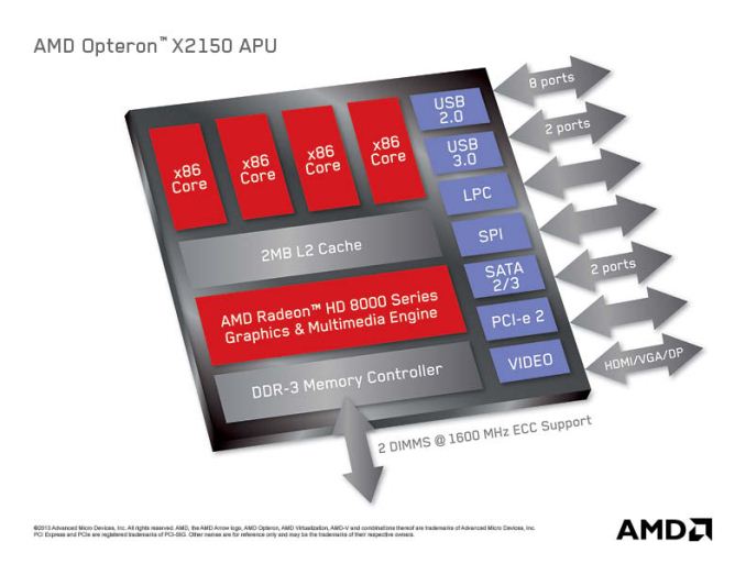
Today, AMD announced that Kabini would make its way into servers in the form of an SoC codenamed Kyoto and under the Opteron brand. The Opteron X1150 CPU and X2150 APU are both quad-core Jaguar SoCs, the main difference between the two is that the X2150 has its Radeon 8000 series GPU enabled while the X1150 is CPU-only. We'll be seeing more solutions in servers with processor graphics enabled going forward, especially given how competent these integrated GPUs are at non-gaming workloads.

AMD boasts better CPU performance (single and multithreaded) than Intel's current 32nm Centerton Atom server platform, which is quite believable given what we've seen from Kabini vs. Atom.
The Kyoto parts are BGA-only, but come with extremely attractive pricing. The X2150 carries a $99 MSRP, while the X1150 is priced at $69. TDPs range between 9 - 17W (depending on CPU clock) on the X1150 with a 2GHz max CPU clock and 11 - 22W on the X2150 with a slightly lower 1.9GHz max CPU clock.
AMD Kyoto Offerings |
|||||||||||||||||||||
CPU Cores |
CPU Configurable Frequency |
GPU Cores |
GPU Configurable Frequency |
TDP Range |
1Ku Pricing |
||||||||||||||||
Opteron X1150 |
4 |
Up to 2.0GHz |
- |
- |
9 - 17W |
$64 |
|||||||||||||||
Opteron X2150 |
4 |
Up to 1.9GHz |
128 |
266 - 600MHz |
11 - 22W |
$99 |
|||||||||||||||
Although not immediately related, Andrew Feldman included this slide in his presentation on Kyoto. I like it a lot so I thought I'd share it here:

In my last Kabini piece I mentioned the two non-negotiables in PC pricing, the cost of the Windows license and the cost of the Intel CPU. As the market puts even more pressure on PCs to reduce pricing, even Microsoft and Intel are forced to look for ways to maintain their margins. Once great partners, those two are presently eyeing each other's lunch.


Read More ...
Toshiba Portege Z10t is a New Take on Convertibles
Convertibles that can jump between being tablets and full-on notebooks are becoming an increasingly popular option due to both the design of Windows 8 and, to a greater extent, the gradual convergence between those product types. We're not quite at the point where anyone has nailed it without making some kind of serious sacrifice, but we're definitely getting there and the experimentation by different vendors is nothing if not interesting.
Enter Toshiba's Portege Z10t. Unlike most full x86 tablets currently available, which use either Intel's current-generation Atom (thus sacrificing performance) or 17W Ivy Bridge (thus sacrificing weight and heat), the Z10t is coming out of the gate with 13W Ivy Bridge. It also includes 4GB of DDR3, a minimum 128GB SSD, and per its business-class design, supports vPro.

Where the Portege's convertible design differs is in the design of the keyboard dock; it's weighted in the back with additional ports and designed to easily close like an ultrabook, but there's no additional battery inside the dock itself. Toshiba will also be offering a separate port-replicator dock to use with the Z10t.
The tablet half is 0.53" thick and weighs a hair under two pounds; with the ultrabook keyboard dock, that weight goes up to a still svelte 3.1 pounds. It's expected to be available soon starting at $1,499.
Read More ...
OPPO Find 5 Review
The Android landscape of today is dominated by a handful of different product lines - Galaxy, Nexus, One, Optimus - both in terms of marketshare as well as mindshare. So it’s nice to be sent a smartphone from a smaller device OEM, particularly one with top shelf specs, a good design, and an interesting plan for actually selling it.
And such arrives the OPPO Find 5. The 5 in the name refers to the 5” 1080p display, which you’ll notice is roughly the same as what you’ll find in the HTC Butterfly and Droid DNA, Sony’s Xperia Z and ZL, the ASUS Padfone Infinity, and a handful of other notable devices from ZTE (Grand S), Huawei (Ascend D2), and LG (Optimus G Pro, Japanese variant). And like the HTC and Sony handsets, the Find 5 comes with Qualcomm’s APQ 8064 SoC, which features four Krait cores clocked at 1.5GHz and an Adreno 320 GPU. Also exciting is the pentaband DC-HSPA+ and the fact that OPPO is offering the Find 5 up for sale on their website in fully unlocked, contract-free form (third-party resellers are also selling it on Amazon). Pricing starts at $499 for the 16GB model, with a 32GB SKU commanding an extra $70. On paper, this is a device that I’ve been excited for since I caught wind of it late last year. How does it hold up in the glass and plastic? Read on to find out.
Read More ...
A Quick Look at the White Nexus 4
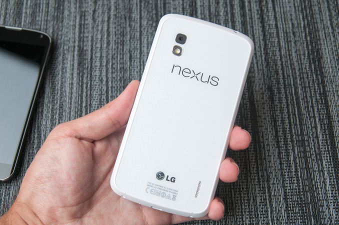
The White Nexus 4 is identical internally to the black Nexus 4 which we reviewed a while back. It's still the same 1.5 GHz APQ8064 inside with 2 GB of LPDDR2 and beautiful 4.7-inch 1280x768 display. The White Nexus 4 we got ahold of came with 16 GB of NAND onboard as well, though there's nothing preventing an 8 GB variant from appearing. All that's different is that now it's a beautiful stark white on the backside with chrome trim everywhere there was black. The front side of the white Nexus 4 remains black, this new model includes white trim around the edge and again white on the back while still including the reflective and faceted structured pattern. It's a purely aesthetic change which – to me at least – looks amazing in person. It's another option which doesn't do anything to sway potential phone shoppers to the Nexus 4 but does refresh the product with a somewhat new look. LG recently made a May 29th date public for the white Nexus 4's availability, there's no official word from Google about when we can expect it to hit the Play Store but release seems imminent. I would expect pricing to be the same for the white version as the black version.
Included with the white Nexus 4 is a white bumper as well, which looks great contrasting with the black Nexus 4 or on the natively white Nexus.
Also our white Nexus 4 came running Android 4.2.2, there's no secret 4.3 or other release running on the hardware we were sampled.


Read More ...
Lian Li PC-TU100 Mini-ITX Case Review
A year and a half ago, we reviewed Lian Li's PC-TU200, a decent but flawed portable enclosure. Has Lian Li improved on that design with the PC-TU100?
Read More ...
NVIDIA GeForce GTX 780 Overclocking Results
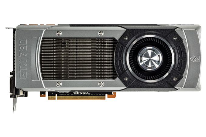
When it comes to overclocking, GTX 780 is in an interesting spot. On the one hand it’s already the highest clocked GK110 part, with a base clock of 863MHz, making it the GK110 part closest to any practical clockspeed limits. On the other hand GTX 780 is built against the same power delivery requirements as GTX Titan, with a stock TDP limit of 250W. This is significant because GTX 780 packs a GPU with fewer enabled SMXes than GTX Titan, and perhaps more importantly half as many RAM chips.
So while GTX 780 can’t necessarily clock any higher than GTX Titan, the additional TDP headroom means that it’s more likely to reach its higher boost bins more often, making overclocking more effective. Compounding all of this is the fact that at stock GTX 780 is more often temperature limited than it is TDP limited, amplifying the factor we have the greatest control over (the temperature throttle) and minimizing the factor we have the least control over (the TDP limit).
GeForce GTX 780 Overclocking |
||||
Stock |
Overclocked |
|||
Core Clock |
863MHz |
1063MHz |
||
Boost Clock |
902MHz |
1102MHz |
||
Max Boost Clock |
1006MHz |
1228MHz |
||
Memory Clock |
6GHz |
7GHz |
||
Max Voltage |
1.162v |
1.2v |
||
And what do we get for our efforts? In short, thanks to the fact that GTX Titan is only 11% faster than GTX 780 on average in the first place, GTX 780 can easily exceed Titan’s stock performance when overclocked. Actual scaling depends on the game – not every game scales well with higher clockspeeds alone – but in most games we at least pick up the 17% lower bound that comes with the memory overclock. This means that an overclocked GTX 780 crosses those few 60fps thresholds that the stock GTX 780 fell just shy of, including the minimum framerate in HItman: Absolution, and the average framerate in Crysis 3.


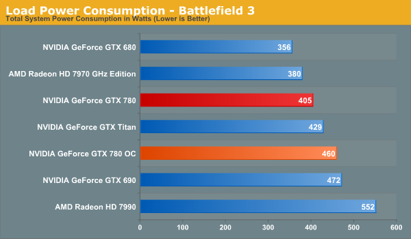


Wrapping things up, when it comes to overclocking the GTX 780 we’re looking at a 17% average performance improvement for a 55W increase in at-the-wall power consumption and 6.3dB increase in noise. This is enough to not only equalize GTX 780 and GTX Titan, but is enough to push GTX 780 ahead by 6% in all of our benchmarks at 2560. Whether it’s worth it is ultimately an individual decision, but in general this is a fairly reasonable tradeoff, especially if the additional noise isn’t a great concern.
Read More ...
Synology Launches DS1813+ Quad-GbE 8-bay NAS
A few weeks back, we had the launch of the DS1513+ 5-bay NAS from Synology. Today, we have the follow-up product in the 8-bay DS1813+. Similar to the DS1513+, we have four GbE ports in the new unit. The base platform remains the same (a 2.13 GHz Atom D2700 CPU and 2 GB of RAM, with the memory being upgradable to
With all four links aggregated, Synology claims up to 350 MBps reads and 200 MBps writes. This is the same as what was claimed for the DS1513+. Other features available in the DS1513+ (such as Synology High Availability, screwless drive bays etc.) are also available in this new unit.


The total capacity can be extended from 8-bays to 18-bays using two DX513 expansion units. This unit is quite attractive to consumers looking for a 8-bay unit, with the only obvious issue being lackluster encryption performance (the Atom D2700 doesn't have the AES-NI feature to accelerate encrypted volume performance).
The unit is now shipping globally, though availability may vary by region. Going by what the DS1812+ was launched at, this unit can be expected to cost slightly north of $1000.
Read More ...
Western Digital Launches WD Se Hard Drive Lineup for Datacenters and High-end NAS Units
One of the most interesting launches from Western Digital last year was the WD Red line of hard drives from the client storage division. It was intended for low to mid-range NAS units (and WD wanted to make sure that it wasn't used for units with more than 5 bays). Today, the Datacenter Storage Business Unit is launching the WD Se line intended for high end NAS units and, more importantly, datacenters looking for scalable storage (i.e, reliable storage which doesn't cost an arm and a leg for scenarios where capacity, rather than performance, is of primary importance).


Read More ...
Nixeus NX-VUE30 30" : A $699 WQXGA (2560x1600) IPS Monitor
Updated: The article's title has been updated at 9:45 PM on 28th May, 2013 to reflect the fact that the monitor has a CCFL backlight. Apologies for the confusion.
In August 2012, Nixeus launched the VUE27, a 27" WQHD (2560x1440) S-IPS LED monitor with a $430 price tag. By providing US-based service / warranty, they managed to win over quite a big segment of the market which was being served by eBay sellers based in Korea. In addition to undercutting the price, the Nixeus unit also provided a wider variety of input ports. Our review found it to be a very decent performer for the price.

The claimed specifications of the NX-VUE30 are as below:
Display Size: 30"
Resolution: 2560*1600 @ 60 Hz
Aspect ratio: 16: 10
Brightness: 350 cd/m2
Contrast Ratio: 1000: 1
Response Time: 7ms (Gray to Gray)
Viewing Angle: 178(H)178(V)
Display Color: 1.07 billion
Stereo Speakers
Connectivity: VGA, HDMI, DL-DVI, Display Port 1.2
Power Power Consumption: <130W
Operation Voltage: 100-240V AC 60/50Hz
Accessories: DL-DVI Cable, Power Cord, User Manual, 3.5mm Audio Cable
Product Dimensions (L x H x D)
27" x 19" x 2.5" w/o Stand
27" x 22" x 2.5" w/ Stand
The unit will launch on
Read More ...
HP Spectre XT TouchSmart Ultrabook Review
HP offers another premium ultrabook experience with a 1080p IPS touch-enabled display, but is it everything it could be?
Read More ...
The Kabini Deal: Can AMD Improve the Quality of Mainstream PCs with Its Latest APU?
There are two non-negotiables in building a PC these days: the cost of Intel silicon and the cost of the Windows license. You can play with everything else but Intel and Microsoft are going to get their share. Those two relatively fixed costs in the PC bill of materials can do one of two things: encourage OEMs to skimp on component cost elsewhere, or drive the entire ecosystem to supply higher quality components at lower prices. If you’ve been following the PC industry for the past decade, I think we’ve seen more of the former and less of the latter.
Apple occupying the high-end of the notebook PC space has forced many OEMs to reconsider their approach, but that’s a more recent change. What AMD seems to offer is an easier path. AMD will take less of the BoM, allowing OEMs to invest those savings elsewhere - a move Intel will never make. Given how much pressure the PC OEMs have been under for the past few years, AMD’s bargain is more appealing now than it has ever been.
With Llano and Trinity, AMD’s story was about giving up CPU performance for GPU performance. With Kabini, the deal is more palatable. You only give up CPU performance compared to higher priced parts (you gain performance compared to Atom), and you get much lower power silicon that can run in thinner/lighter notebooks. Typically at the price points Kabini is targeting (sub-$400 notebooks), you don’t get pretty form factors with amazing battery life. AMD hopes to change that.
Read More ...
Mythlogic Callisto 1512 (Clevo W550EU) Ultrabook Review
Major OEMs are producing ultrabooks at a breakneck pace, but vendors like Clevo are making sure boutiques can get in on the market, too. Mythlogic sent us their Callisto 1512 based on the Clevo W550EU for testing.
Read More ...
Report: Apple Signs Deal with Warner Music Group for "iRadio"
iRadio is expected to make an appearance at WWDC next week
     |
Read More ...
Motorola Wants to Use Tattoos, Pills Instead of Smartphone Passwords
But will consumers want to use them?
| |
Read More ...
Chinese Solar Firms Caught Using Substandard Materials
Panels age and break prematurely
| |
Read More ...
Gmail Gets New Tab-Style Overhaul
Users can have up to five categorized tabs
| |
Read More ...
Amazon Eliminates Use of Multiple Passwords Using "Login with Amazon"
Amazon customers can sign-in to apps, websites and games using their Amazon login information
| |
Read More ...
Quick Note: Office 365 Home Premium Hits 1 Million Subscribers in Just Over 100 Days
It's the best-selling version yet
| |
Read More ...
Texas Aims to Become the First State With Strong Email Privacy Protections
Bill to put an end to warrantless federal prying into citizen email data
| |
Read More ...
AMD Debuts Jaguar-Based Opteron X-Series, With Onboard GCN GPU
New chips use "Jaguar" CPU cores and Graphics Core Next GPU cores
| |
Read More ...
Tim Cook Doesn't Care if Android is Beating iOS in Sales
Apple's chief hints at new products -- iWatch, smart TV -- plus talks taxes, Lisa Jackson hiring, and lawsuits
| |
Read More ...
Available Tags:Gigabyte , Xeon , Server , Motherboards , AMD , Toshiba , NVIDIA , GeForce , GTX , Western Digital , HP , Apple , Motorola , Smartphone , Gmail , Amazon , GPU , Android , iOS ,
No comments:
Post a Comment