
The GeForce GTX 660 Ti Review, Feat. EVGA, Zotac, and Gigabyte
NVIDIA has a bit of a problem right now: their products are a bit too popular. Between the GK104-heavy desktop GeForce lineup, the GK104 based Tesla K10, and the GK107-heavy mobile GeForce lineup, NVIDIA is selling every 28nm chip they can make. As a result NVIDIA has been unable to expand their market presence as quickly as customers would like. For the desktop in particular this means NVIDIA has a very large, very noticeable hole in their product lineup between $100 and $400, which composes the mainstream and performance market segments.
Long-term NVIDIA needs more production capacity and a wider selection of GPUs to fill this hole, but in the meantime they can at least begin to fill it with what they have to work with. This brings us to today’s product launch: the GeForce GTX 660 Ti. With nothing between GK104 and GK107 at the moment, NVIDIA is pushing out one more desktop product based on GK104 in order to bring Kepler to the performance market. Serving as an outlet for further binned GK104 GPUs, the GTX 660 Ti will be launching today as NVIDIA’s $300 performance part.

 |  |
Read More ...
Xiaomi Announces MIUI Phone Mi-Two with Quad Core Krait APQ8064 inside
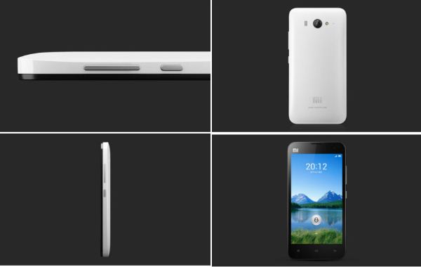
Today Xiaomi announced its Mi-Two handset, which includes a 1.5 GHz Qualcomm Snapdragon S4 Pro APQ8064 SoC and 2 GB of LPDDR2 RAM. Though there have been leaks and rumors about other phones in develoment based around APQ8064, this is to my knowledge the first handset officially announced with the quad core Krait (and Adreno 320) SoC inside. Xiaomi has priced the Mi-Two at 1999HKD which works out to 315USD for comparison.


| Xiaomi Mi-One and Mi-Two Comparison | |||||
| Device | Mi-One | Mi-Two | |||
| SoC | 1.5 GHz MSM8x60 (Dual core Scorpion + Adreno 220) | 1.5 GHz APQ8064 (Quad core Krait + Adreno 320) | |||
| RAM/NAND/Expansion | 1 GB LPDDR2, 4 GB NAND, microSD | 2 GB LPDDR2, 16 GB NAND, microSD | |||
| Display | 4.0" 854x480 | 4.3" IPS 1280x720 | |||
| Network | WCDMA (14.4) / GPRS / EDGE / (1x+EVDO if MSM8660) | DC-HSPA+ (42.2) / GPRS / EDGE | |||
| Dimensions | 125mm x 63mm x 11.9mm | 126mm x 62mm x 10.2mm | |||
| Camera | 8 MP | 8 MP 5P F/2.0 | |||
Xiaomi doesn't pull any punches and directly compares the Mi-Two to the competition from HTC and Samsung in their slides. I've gathered almost all of them up into a gallery for your perusal. It's great to see Xiaomi going into this level of detail about their handset.


Update: The Xiaomi Mi-Two page is now live and includes a bit more detail, including band support, which is WCDMA 850, 1900, 2100 alongside quad band GSM. There's also a small note about the Mi-Two having antenna diversity. The pages also note that the Mi-Two will go on sale in October for 1999HKD.
Xiaomi also made their slide deck from the presentation live after some time, I've exported the slide deck pages to a gallery as well.


Sources: Xiaomi (microblogging), Twitter, Xiaomi (Mi-Two Page)
| |
Read More ...
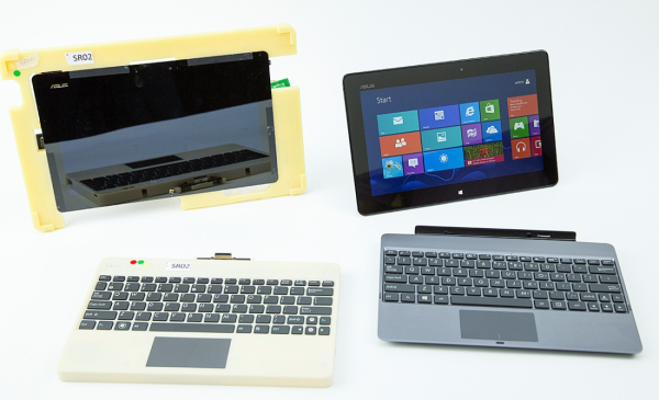
Samsung Series 7 NP700Z7C Review
We recently posted our first look at Dell’s new XPS 15, a Windows-focused laptop that took more than a few design elements of the standard MacBook Pro 15. While there was plenty to like with the design and features, we’re still waiting for a final BIOS fix that will hopefully address the throttling issues many have experienced with the laptop. Today, we have a notebook from Samsung that’s very similar in many areas to the XPS 15, only it’s in a larger 17.3”-screen chassis and has slightly faster components.

| |
Read More ...
Intel Brings TRIM to RAID-0 SSD Arrays on 7-Series Motherboards, We Test It
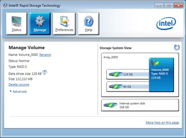
As soon as I got confirmation from Intel, I fired up a testbed to confirm the claim. Before I get to the results, let's have a quick recap of what all of this means.
Why does TRIM Matter?
The building block of today's SSDs that we love so much is 2-bit-per-cell MLC NAND Flash. The reason that not all SSDs are created equal is because of two important factors:1) Each NAND cell has a finite lifespan (determined by the number of program and erase cycles), and
2) Although you can write to individual NAND pages, you can only erase large groups of pages (called blocks)
These two factors go hand in hand. If you only use 10% of your drive's capacity, neither factor is much of an issue. But if you're like most users and run your drive near capacity, difficulties can arise.
Your SSD controller has no knowledge of what pages contain valid vs. invalid (aka deleted) data. As a result, until your SSD is told to overwrite a particular address, it has to keep all data on the drive. This means that your SSD is eternally running out of free space. Thankfully all SSDs have some percentage of spare area set aside to ensure they never actually run out of free space before the end user occupies all available blocks, but how aggressively they use this spare area determines a lot.
Aggressive block recycling keeps performance high, at the expense of NAND endurance. Conservative block recycling preserves NAND lifespan, at the expense of performance. It's a delicate balance that a good SSD controller must achieve, and there are many tricks that can be employed to make things easier (e.g. idle time garbage collection). One way to make things easier on the controller is the use of the ATA TRIM command.
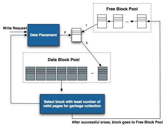
The SSD doesn't have to take immediate action upon receiving the TRIM command for specific LBAs, but many do. By knowing what pages and blocks no longer contain valid data, the SSD controller can stop worrying about preserving that data and instead mark those blocks for garbage collection or recycling. This increases the effective free space from the controller's perspective, and caps a drive's performance degradation to the amount of space that's actively used vs. a continuing downward spiral until the worst case steady state is reached.
TRIM was pretty simple to implement on a single drive. These days all modern SSDs support it. It's only if you have one of the early Intel X25-M G1s that you're stuck without TRIM. Drives that preceded Intel's X25-M are also TRIMless. Nearly all subsequent drives we recommended either had TRIM support enabled through a firmware update or had it from the start.
Enabling TRIM on a RAID array required more effort, but only on the part of the storage driver. The SSD's firmware and OS remain unchanged. Intel eventually added TRIM support in its RAID drivers for RAID-1 (mirrored) arrays, but RAID-0 arrays were a different story entirely. There's a danger in getting rid of data in a RAID-0 array, if a page or a block gets TRIMed on one drive that's actually necessary, the entire array can be shot. There was talk of Intel enabling TRIM support on RAID-0 arrays as early as 2009, but given the cost of SSDs back then not many users were buying multiple to throw in an array.
The cost of SSDs has dropped considerably in the past 4 years. The SSD market is far more mature than it used to be. Intel isn't as burdened with the responsibility of bringing a brand new controller and storage technology to market. With some spare time on its hands, Intel finally delivered a build of its RAID drivers that will pass the ATA TRIM command to RAID-0 arrays.
The Requirements
The requirements for RAID-0 TRIM support are as follows:A 7-series motherboard (6-series chipsets are unfortunately not supported).
Intel's Rapid Storage Technology (RST) for RAID driver version 11.0 or greater (11.2 is the current release)
Windows 7 (Windows 8 support is forthcoming)
The lack of support for 6-series chipsets sounds a lot like a forced feature upgrade. Internally Intel likely justifies it by not wanting to validate on older hardware, but I don't see a reason why TRIM on RAID-0 wouldn't work on 6-series chipsets.
I am not sure if TRIM will work on RAID-10 arrays. I'm going to run some tests shortly to try and confirm. Update: I don't believe it works on RAID-10 arrays. I'm still running tests to confirm but so far it looks like the answer is no.
Testing TRIM on RAID-0

The 64GB Samsung SSD 830 is good for almost 500MB/s in sequential reads and under 160MB/s sequential writes. Two of them in RAID-0 should be able to deliver over 1GB/s of sequential read performance and over 300MB/s in sequential writes. A quick pass of HDTach confirms just that:

For the control run I used Intel's 10.6 RST drivers (10.6.0.1022). I filled the array with sequential data, then randomly wrote 4KB files over the entire array at a queue depth of 32 for 30 minutes straight. I formatted the array (thus TRIMing all LBAs) and ran an HD Tach pass to see if performance recovered. Remember if the controller was told that all of its data was invalid, a sequential write pass would run at full speed since all data would be thrown away as it was being overwritten. Otherwise, the controller would try to preserve its drive full of garbage data as long as possible.
The 10.6 RST drivers don't pass TRIM through to RAID-0 arrays, and the results show us just that:

Here's what the pass looks like after the same fill, torture, TRIM, HD Tach routine with the 11.2 drivers installed:

Bringing TRIM support to RAID-0 arrays provides users with a way of enjoying next-gen SSD performance sooner rather than later, without giving up an important feature. Pretty much all high-end SSDs are capped to 6Gbps limits when it comes to sequential IO. Modern SATA controllers deliver 6Gbps per port, allowing you to break through the 6Gbps limit by aggregating drives in RAID.
The only negative here is that Intel is only offering support on 7-series chipsets and not on previous hardware. That's great news for anyone who just moved to Ivy Bridge and has a RAID-0 array of SSDs, but not so great for everyone else. A lot of folks supported Intel over the past couple of years and Intel has had some amazing quarters as a result - I feel like the support should be rewarded. While I understand Intel's desire to limit its validation costs, I don't have to be happy about it.
For more information on how SSDs work, check out our last major article on the topic.
| |
Read More ...
Live from Samsung's Galaxy Note 10.1 Launch
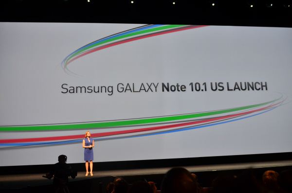

Samsung got Moulin Rouge director Baz Luhrmann on stage to talk about his experience with the Galaxy Note 10.1. Ultimately Samsung is touching on a major issue with tablets today: the inability to enjoy the same level of productive multitasking we have on traditional PCs and notebooks.


I do feel that Windows 8/RT based tablets will ultimately address a lot of what Samsung has been trying to do with Android over the past couple of years. The real question is whether or not Samsung will bring a lot of its Android experiments to Windows RT later this year.
The Galaxy Note 10.1 will be available for purchase starting tomorrow, priced at $499 for the 16GB WiFi model and $549 for the 32GB WiFi model (white and dark gray colors available). The tablet comes preloaded with Adobe's Photoshop Touch software that's optimized for use with the bundled S Pen.
| Android Tablet Specification Comparison | ||||||
| ASUS Eee Pad Transformer Prime | ASUS Transformer Pad Infinity | Google Nexus 7 | Samsung Galaxy Note 10.1 | |||
| Dimensions | 263 x 180.8 x 8.3mm | 263 x 180.6 x 8.4mm | 198.5 x 120 x 10.45mm | 262 x 180 x 8.9mm | ||
| Chassis | Aluminum | Aluminum + Plastic RF Strip | Plastic | Plastic | ||
| Display | 10.1-inch 1280 x 800 Super IPS+ | 10.1-inch 1920 x 1200 Super IPS+ | 7-inch 1280 x 800 IPS | 10.1-inch 1280 x 800 | ||
| Weight | 586g | 594g | 340g | 597g | ||
| Processor | 1.3GHz NVIDIA Tegra 3 (T30 - 4 x Cortex A9) | 1.6GHz NVIDIA Tegra 3 (T33 - 4 x Cortex A9) | 1.3GHz NVIDIA Tegra 3 (T30L - 4 x Cortex A9) | 1.4GHz Exynos 4 (4 x Cortex A9) | ||
| Memory | 1GB | 1GB DDR3-1600 | 1GB | 2GB | ||
| Storage | 32GB/64GB + microSD slot | 32/64GB + microSD slot | 8/16GB | 16/32GB + microSD slot | ||
| Battery | 25Whr | 25Whr | 16Whr | 26Whr | ||
| OS | Android 4.0 | Android 4.0 | Android 4.1 | Android 4.0 | ||
| Pricing | $499/$599 | $499/$599 | $199/$249 | $499/$549 | ||
| |
Read More ...
Microsoft Reveals First Battery Life Specs for Windows RT Tablets
The OS is final as of now, but there's still a lot of work being done on drivers. I don't expect to see anything resembling final drivers until early October. That being said, Microsoft did share a bit of early data about the first Windows RT tablets:
| Windows RT Launch Tablet Specification Range | |||||
| Min | Max | Apple iPad (2012) | |||
| HD Video Playback at 200 nits | 8 hours | 13 hours | 11.15 hours | ||
| Connected Standby | 320 hours | 409 hours | - | ||
| Battery Capacity | 25 Wh | 42 Wh | 42 Wh | ||
| Screen Size | 10.1-inches | 11.6-inches | 9.7-inches | ||
| Weight | 520 g | 1200 g | 652 g | ||
| Length | 263 mm | 298 mm | 241.2 mm | ||
| Width | 168.5 mm | 204 mm | 185.7 mm | ||
| Height | 8.35 mm | 15.6 mm | 9.4 mm | ||
It's disappointing to see a lack of commentary on battery life stressing more than just the video decode logic on the SoC and display. I'm also interested to see how Atom based Clovertrail Windows 8 tablets stack up against these Windows RT devices in terms of battery life and performance. If Atom based Windows 8 tablets can deliver a comparable experience there, and are comparably priced (which seems to be the case based on what I heard at Computex), then the choice between RT and Atom based Windows 8 tablets may boil down to whether free Office or legacy compatibility matter more to you.
| |
Read More ...
OWC Announces 480GB SSD Upgrade for MacBook Pro with Retina Display
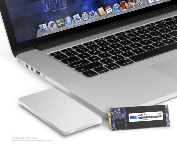
Today, as expected, OWC announced its 480GB Mercury Aura Pro upgrade for the Retina MacBook Pro. The SandForce SF-2281 based SSD is priced at $579.99, which actually doesn't save you any money compared to buying the upgraded configuration directly from Apple. OWC's route does offer a couple of benefits however: 1) customers who order before September 30th will receive a USB 3.0 enclosure that will let you use your old 256GB SSD as an external drive (the enclosure costs $60 separately, and you still get to use your 256GB SSD), and 2) if you've already purchased a 256GB rMBP and later discover that you need more storage simply buying the $2799 model isn't an option, making the Mercury Aura Pro a viable option.
A quick search of 480GB SF-2281 based drives reveals that many are still priced over $500, although it's still possible to get some drives at lower price points. NAND pricing tends to be highly volatile, not to mention the benefits that having a direct relationship with a fab offers, both of which contribute to the wide spread.
The other thing to keep in mind with any SF-2281 based SSD is the difference in performance between compressible and incompressible data. If you're running FileVault on your rMBP you will see lower performance from anything SandForce based compared to the standard Samsung PM830 used in the stock rMBP.
All of that being said, it's great to see OWC offer an upgrade path for the MacBook Pro with Retina Display. Pre-orders for the Mercury Aura Pro are available immediately, with first shipments going out on or around August 21.
| |
Read More ...
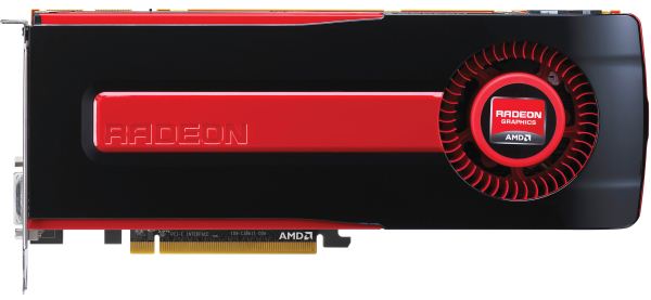
AMD Announces New, Higher Clocked Radeon HD 7950 with Boost
August is not typically a busy time of the year for the GPU industry. But this is quickly turning out to be anything but a normal August. Between professional and consumer graphics cards we have a busy week ahead.
Kicking things off on the consumer side today, AMD is announcing that they will be releasing a new Radeon HD 7950 with higher clockspeeds. The new 7950, to be called the Radeon HD 7950, is a revised version of the existing 7950 that is receiving the same performance enhancements that the 7970 received back in June, which were the basis of the Radeon HD 7970 GHz Edition.
| |
Read More ...
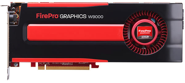
The AMD FirePro W9000 & W8000 Review: Part 1
Despite the wide range of the GPU coverage we do here at AnandTech, from reading our articles you would be hard pressed to notice that AMD and NVIDIA have product lines beyond their consumer Radeon and GeForce brands. Consumer video cards compose the bulk of all video cards shipped, the bulk of revenue booked, and since they’re targeted at a very wide audience, the bulk of all marketing attention. But that doesn't mean they're the only video cards that matter.
Abutting the consumer market is the smaller, specialized, but equally important professional market that makes up the rest of the desktop GPU marketplace. Where consumers need gaming performance and video playback, professionals need compute performance, specialized rendering performance, and above all a level of product reliability and support beyond what consumers need.
| |
Read More ...
The AnandTech Podcast: Episode 1
This marks our first ever official AnandTech podcast. The plan is to regularly do more of these and my hope is to be able to rope in all of the AnandTech writers to spend some time on the mic. We're getting an RSS feed for the podcast setup but for now here are direct links to the first episode (mp3 and m4a formats) as well as an embedded player here if you want to get started immediately. The total play time is just over 1 hour (01:01:05) and that will likely be our target going forward. As always, comments are welcome and appreciated. Let us know what you liked, hated and want to hear more of.
| |
Read More ...
ASUS P8Z77-V Premium Review: A Bentley Among Motherboards
In the car industry, there is a large variety of cars to choose from - both the cheap and the expensive will get you from A to B, but in various amounts of luxury, with different engines and features under the hood. In comparison the motherboard industry, we have nothing like this - products are built to specifications and have to remain price competitive. Very rarely do we get a price competitive motherboard with a ton of features that also stretches the wallet in the same way a luxury car might do. For this analogy, we have the P8Z77-V Premium from ASUS to review, which comes in at $450 MSRP, but features Thunderbolt connectivity, dual Intel NIC, an onboard 32GB mSATA SSD, a PLX chip for 4-way PCIe devices, onboard WiFi, Bluetooth, and extra SATA/USB ports.

| |
Read More ...
RightWare Launches Basemark GUI Free on Android Market - We Test It Out

Basemark GUI Free includes both the Vertex and Blend subtests, which are designed to test different areas of OpenGL ES 2.0 performance on Android devices. We're no stranger to this test, having seen it in original form a while ago. New and improved functionality in this version includes an offscreen version of each subtest which runs at 720p in addition to the native resolution run. The offscreen run displays small tiles of the currently rendered scene to verify that the scene is being drawn, just like GLBenchmark does. Results also get uploaded to RightWare's PowerBoard and presented (for example, see this HTC One X result page) alongside RightWare's other data. Check out the gallery for screenshots from the entire application. I should note that there's also a video of the full Basemark GUI run back in my original launch story.
The Vertex and Blend subtests haven't changed at all since we originally saw them, but I'm reproducing RightWare's description of the tests in full below to give an idea what the workload is for each part. In general, Basemark GUI is a much more challenging and modern workload compared to Basemark ES 2.0, though it ends up being heavy on its geometry payload thanks to the Vertex test.


Vertex Test:
The Vertex test loads vertex data from the disk, loads it into vertex buffers, displays the geometry and then discards unnecessary data after a frame has been rendered.Blend Test:
The Vertex test contains several load cycles of increasing complexity. A cycle contains a preprocessing step that is not scored, and the final scoring stage. The geometry is composed of 10 distinct city blocks which are each approximately 3000 triangles and 6000 vertices in size. In the preprocessing stage, a city layout is generated out of the blocks based on the complexity requirements of a specific cycle. The entire layout is then saved to disk into an indexed binary file. Although visually similar, each block has its own unique location in this file. Identical blocks are textured using the same texture which resides in the GPU memory throughout the test.
Once the actual scoring run starts, the city is moved towards the camera. Blocks that disappear beyond the plane of view are discarded from the memory. New blocks appearing at the visible horizon are read from the disk.
The test load is increased incrementally to a maximum load. The test load ranges from approximately 3k vertices per frame to 15k vertices per frame. The number of triangles on the screen ranges from 190k to 250k.
The scene geometry is rendered using a single texture material and fog. There are two lights. The OpenGL ES 2.0 shaders use per vertex lighting.

The Blend test measures the efficiency of alpha blended rendering on the platform. Blending combines the incoming source fragment’s RGBA values with the RGBA values in the destination fragment stored in the frame buffer at the fragment’s x,y location. The active blend equation calculates the final RGBA value at the location from the input values. Overlay of graphical elements is a critical component of composition operations.
Overlay draw renders a large set of simple primitives. The number of overlain primitives will increase through the duration of the test up to a maximum specified count. The test is rendered twice: First with front-to-back ordering of the image planes and then with back-to-front ordering.

I've gone ahead and run Basemark GUI Free on a fairly representative combination of devices, same as what I did in the GLBenchmark 2.5 piece, for comparison.
Here we have two Samsung SoCs paired with the ARM Mali-400 MP4 GPU: the original dual-core Exynos 4210 as well as the Exynos 4 Quad (4412) from the international Galaxy S 3 which we're reviewing. Tegra 3 makes an appearance in the HTC One X International, as does TI's OMAP 4460. The latter shows up in two configurations, one with the SGX 540 running at full 384MHz clocks in the Huawei Ascend P1 and another with the SGX 540 running at 307MHz in the Galaxy Nexus (CPU clocks are 20% lower as well in the Galaxy Nexus). Finally we have Qualcomm's dual-core Snapdragon S4 with its Adreno 225 GPU in the HTC One X and the US Galaxy S 3, and Adreno 205 inside the HTC One V which I tossed in as well.

In the offscreen tests, both Adreno and Tegra 3 do very well, posting impressive numbers. In addition, SGX540 does surprisingly well. What's surprising is to see the Exynos based SoCs not do as well here, until you realize that the Vertex test is (hence the name) strongly dominated by vertex data, it isn't the kind of shader compute test we're used to seeing with GLBenchmark. Recall that Mali-400 isn't a unified shader architecture, and explicitly features more pixel shader hardware than vertex shader hardware.
Because the end score (in FPS) for on and off screen is the average of both subtest scores, it's hard to be completely certain that the large vertex workload is the reason for Mali-400MP4 doing how it does in the above tests, but it's a logical conclusion. Of course, the licensed version of Basemark GUI not on the Play Store does expose data from individual subtests.

Unlike Basemark ES 2.0 Taiji Free, Basemark GUI Free includes that offscreen 720p test, which makes it a much more functional tool for end user comparison across devices. I'm told that future RightWare benchmarks in the Play Store will also include offscreen subtests, which is a great step in the right direction.
Source: Google Play Store (Basemark GUI Free), PowerBoard (HTC One X)
| |
Read More ...
HP 2311xi IPS Monitor
HP managed to make the right choices with their 27” ZR2740w monitor, hitting a reasonable price point without sacrificing quality. Now HP has introduced their 2311xi monitor, a 23” IPS display with LED backlighting that is designed with value in mind. Even with their value target, they haven't cut back on features, with multiple inputs and a good amount of adjustments available inside of the display.

| |
Read More ...
Samsung Announces A15/Mali-T604 Based Exynos 5 Dual
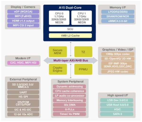
The CPU
Samsung's Exynos 5 Dual integrates two ARM Cortex A15 cores running at up to 1.7GHz with a shared 1MB L2 cache. The A15 is a 3-issue, Out of Order ARMv7 architecture with advanced SIMDv2 support. The memory interface side of the A15 should be much improved compared to the A9. The wider front end, beefed up internal data structures and higher clock speed will all contribute to a significant performance improvement over Cortex A9 based designs. It's even likely that we'll see A15 give Krait a run for its money, although Qualcomm is expected to introduce another revision of the Krait architecture sometime next year to improve IPC and overall performance. The A15 is also found in TI's OMAP 5. It will likely be used in NVIDIA's forthcoming Wayne SoC, as well as the Apple SoC driving the next iPad in 2013.The Memory Interface

TI's OMAP 5 features a 2x32-bit LPDDR2/DDR3 interface and is currently rated for data rates of up to 1066MHz, although I suspect it wouldn't be too much of a stretch to get DDR3-1600 memory working with the SoC. Qualcomm's Krait based Snapdragon S4 also has a dual-channel LPDDR2 interface, although once again there's no word on what the upper bound will be for supported memory frequencies.
The GPU

Video encode and decode are rated at 1080p60.
The Rest
To complete the package Samsung integrates USB 3.0, SATA 3, HDMI 1.4 and eDP interfaces into the Exynos 5 Dual. The latter supports display resolutions up to 2560 x 1600. The complete package is the new face of a modern day mobile system on a chip.Samsung remains very aggressive on the SoC front. The real trick will be whether or not Samsung can convince other smartphone and tablet vendors (not just Samsung Mobile) to use its solution instead of something from TI, NVIDIA or Qualcomm. As long as Samsung Mobile ships successful devices the Samsung Semiconductor folks don't have to worry too much about growing marketshare, but long term it has to be a concern.
| |
Read More ...
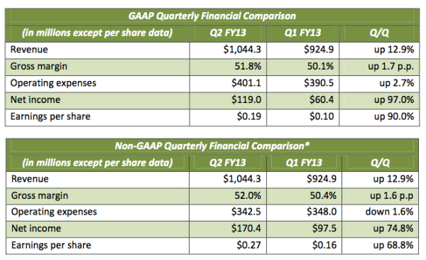
NVIDIA Q2 FY13 Earnings Report: $1.04B Revenue, Tegra Sales Recover
I plotted revenue across all three businesses going back over the past 2.5 years:
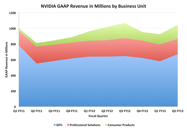
As it stands, Tegra (and the rest of the consumer products group) is responsible for 17.2% of NVIDIA's total quarterly revenue. That's hardly insignificant. If more PCs move over to processor graphics in lieu of discrete GPUs, Tegra will need to grow even more to make up for that loss. I have been concerned about the margins NVIDIA gets out of its Tegra parts. OEMs in the ARM mobile space expect to pay below $30 for close to 100mm2of silicon. As a result, margins on a chip like Tegra are no where near what they are on a high-end GPU. The question is, are they competitive with entry level discrete GPUs? It's still too early to correlate increases in Tegra revenue with an impact on gross margins, but so far there's nothing to complain about:

At the end of the day, NVIDIA had a good quarter and Tegra remains an important part of the business. NVIDIA has a couple of high profile design wins with Tegra 3 in Windows 8 devices later this year, including Microsoft's Surface tablet. The real question is how good will Wayne be next year. What I've heard thus far is promising, but I don't have any hard data yet. I suspect we'll also really begin to see the impact of processor graphics integration next year with Haswell. NVIDIA doesn't break down GPU revenue by market segment so it's unclear how much of a loss the consumer products division would have to cover should more OEMs choose to leave discrete GPUs out of their systems.
The good news for NVIDIA is the high end (and quite profitable) GPU market is likely safe for the near future. The question remains how big of an impact we'll see at the entry level and lower midrange segments. A lot of that really depends on the success of Ultrabooks, Windows 8 tablets and other ultra small form factor machines that may not prioritize discrete GPUs.
For now it's clear the Consumer Products group and Tegra has legs. NVIDIA's margins and revenue have improved over the past two years but there's a lot of room to grow on the back of smartphones and tablets. NVIDIA has done surprisingly well with Tegra over the past couple of years, especially in the face of some very strong qualcompetition. We'll find out soon enough if Wayne has what it takes to give NVIDIA's Consumer Products business its first $200M+ quarter.
| |
Read More ...
The Intel SSD 910 Review
The increase in compute density in servers over the past several years has significantly impacted form factors in the enterprise. Whereas you used to have to move to a 4U or 5U chassis if you wanted an 8-core machine, these days you can get there with just a single socket in a 1U or 2U chassis (or smaller if you go the blade route). The transition from 3.5" to 2.5" hard drives helped maintain IO performance as server chassis shrunk, but even then there's a limit to how many drives you can fit into a single enclosure. In network architectures that don't use a beefy SAN or still demand high-speed local storage, PCI Express SSDs are very attractive. As SSDs just need lots of PCB real estate, a 2.5" enclosure can be quite limiting. A PCIe card on the other hand can accommodate a good number of controllers, DRAM and NAND devices. Furthermore, unlike a single 2.5" SAS/SATA SSD, PCIe offers enough bandwidth headroom to scale performance with capacity. Instead of just adding more NAND to reach higher capacities you can add more controllers with the NAND, effectively increasing performance as you add capacity.

It took surprisingly long for Intel to dip its toe in the PCIe SSD waters. In fact, Intel's SSD behavior post-2008 has been a bit odd. To date Intel still hasn't released a 6Gbps SATA controller based on its own IP. Despite the lack of any modern Intel controllers, its SSDs based on third party controllers with Intel firmware continue to be some of the most dependable and compatible on the market today. Intel hasn't been the fastest for quite a while, but it's still among the best choices. It shouldn't be a surprise that the market eagerly anticipated Intel's SSD move into PCI Express. Read on for our full review of Intel's SSD 910, the company's first PCIe SSD.
| |
Read More ...
Pulse Launches Pulse for Web

The website has a prominent Internet Exporer branding, and Windows 8 & Internet Explorer 10 users can take advantage of some cool multi-touch gestures as well. Users with existing Pulse.me accounts can sign in immediately to find all their sources synced and ready to go. Alternatively, you can create a new account or sign in using Facebook credentials as well.
Pulse has almost exlusively been my favorite newsreader app for quite some time now and the new web-based version makes things even better.
Head on over to Pulse right now and check it out for yourself.
| |
Read More ...
T-Mobile RF Engineer Does Reddit AMA - Answers a Few LTE Questions
In the past, carriers have been guarded if not purposely opaque about things like radio network planning, infrastructure rollouts, and other competitive details. With the smartphone boom well underway, many of those curtains are starting to fall as customers get more and more savvy with air interfaces and asking the important questions. This morning on Reddit, a T-Mobile RF engineer started an AMA,
I obviously could not resist the temptation to ask a few questions myself, and got some interesting replies.
My questions:
- Can you talk briefly about how much traffic on GERAN you see from iPhone customers? How much of a catch-22 is that situation for moving that PCS spectrum dedicated to it over to WCDMA?
- In some markets it seems as though T-Mobile will be unable to run DC-HSDPA on AWS alongside any LTE because of lack of spectrum. Obviously multi-band carrier aggregation (WCDMA carriers on PCS and AWS) is a big part of that future, can you talk about the challenges involved there?
- Will T-Mobile deploy 3GPP Rel 8, or will you guys go right to Rel 10 for LTE?
- How much variance in WCDMA utilization do you see across markets? From your point of view, are caps and the end of unlimited data plans really backed up across the board, or just in a few markets? In my AZ markets (Tucson, Phoenix) where I do a lot of testing, I regularly find I have the sector to myself.
- Traditional PA at bottom architecture, or Remote Radio Head architecture for T-Mobile LTE?
- This is already somewhat obvious, but could you confirm/discuss T-Mobile LTE channel bandwidths?
- We have about a million iPhones on our network now. 99.9% of their traffic is 2G/EDGE only right now, so obviously their load is dwarfed by everything else. The iPhone is a significant part of the modernization project. Once implemented, iPhones will work on U1900 at much higher speeds.
- Spectrum is always a limitation. With the software that exists now, you will not be able to do dual carrier split between AWS and PCS. That's supposed to be fixed in the future, but I don't know a timeline on it.
- It depends on a lot of things. In general, I think caps are stupid, especially the way that we handle them. Events (concerts, sporting events, malls @ Christmas) crush us though.
- We're going with remote radios as much as we can, for LTE, UMTS, and GSM.
- LTE will launch with a single 10 MHz channel, 5 up, 5 down.
Update: The T-Mobile AMA source has dropped a few other interesting tidbits, as the AMA has progressed. Among mundane things like equipment failures, copper theft and vandalism are a major source of problems for T-Mobile in some markets, along with the usual kind of things like animal encroachment. In addition, the source uses a Samsung Galaxy S 3, and noted the use of disguised cell sites.
Source: Reddit
| |
Read More ...
Plextor Releases M5 Pro SSD: Say Hello to Marvell 88SS9187 and 19nm Toshiba NAND

Not only is Plextor using a brand new controller, the M5 Pro is also the first consumer SSD to use Toshiba's 19nm Toggle-Mode MLC NAND.
| Plextor M5 Pro Specifications | |||
| Capacity | 128GB | 256GB | 512GB |
| Controller | Marvell 88SS9187 | ||
| NAND | Toshiba 19nm Toggle-Mode MLC NAND | ||
| Sequential Read | 540MB/s | 540MB/s | 540MB/s |
| Sequential Write | 340MB/s | 450MB/s | 450MB/s |
| 4K Random Read | 91K IOPS | 94K IOPS | 94K IOPS |
| 4K Random Write | 82K IOPS | 86K IOPS | 86K IOPS |
| Cache (DDR3) | 256MB | 512MB | 768MB |
| Warranty | 5 years | ||
| Availability | Mid-August 2012 | ||
Pricing is to be announced but I would expect the M5 Pro to be priced similarly to what the M3 Pro is currently selling for. Exact availability is still unknown but Plextor is saying mid-August 2012 in the press release, so we should see this drive retailing in a few weeks. Our review sample is already on its way here so stay tuned for our review.
| |
Read More ...
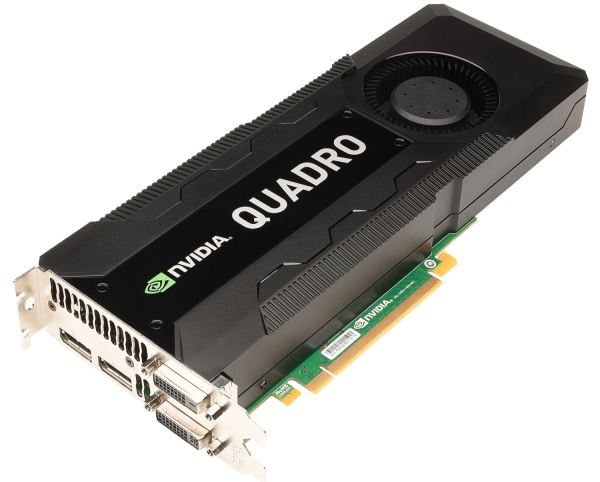
NVIDIA Announces Kepler-Based Quadro K5000 & Second-Generation Maximus
Since the initial launch of NVIDIA’s unusual chip stack for Kepler in late March, there has been quite a bit of speculation on how NVIDIA would flesh out their compute and professional products lines. Typically NVIDIA would launch a high-end GPU first (e.g. GF100), and use that to build their high-end consumer, professional, and compute products. Kepler of course threw a wrench into that pattern when the mid-tier GK104 became the first Kepler GPU to be launched.
The first half of that speculation came to rest in May, when NVIDIA has announced their high-end Kepler GPU, GK110, and Tesla products based on both GK104 and GK110. NVIDIA’s solution to the unusual Kepler launch situation was to launch a specialized Tesla card based on GK104 in the summer, and then launch the more traditional GK110 based Tesla late in the year. This allowed NVIDIA to get Tesla K10 cards in the hands of some customers right away (primarily those with workloads suitable for GK104), rather than making all of their customers wait for Tesla K20 at the end of the year.
Meanwhile the second half of that speculation comes to an end today with the announcement of NVIDIA’s first Kepler-based Quadro card, the Quadro K5000.
| |
Read More ...
AMD Introduces FirePro A300 & A320 APUs: Trinity for Graphics Workstations

One of the first examples of AMD's quick acting is in today's announcement of a new FirePro series of APUs. On the desktop and in mobile we have Trinity based APUs. The FirePro APUs are aimed at workstations that need professional quality graphics drivers but are fine with entry level GPU performance.

Going up against Intel in a market that does value graphics performance meets the agile AMD requirement, although it remains to be seen how much of a burden slower scalar x86 performance is in these workstation applications.
AMD's motivation behind doing a FirePro APU is simple: workstation/enterprise products can be sold at a premium compared to similarly sized desktop/notebook parts. Take the same Trinity die, pair it with FirePro drivers you've already built for the big discrete GPUs, and you can sell the combination for a little more money with very little additional investment. Anything AMD can do at this point to increase revenue derived from existing designs is a much needed effort.
There are two FirePro APUs being announced today, the A300 and A320:
| AMD FirePro APUs | |||||
| APU Model | A300 | A320 | |||
| “Piledriver” CPU Cores | 4 | 4 | |||
| CPU Clock (Base/Max) | 3.4GHz / 4.0GHz | 3.8GHz / 4.2GHz | |||
| L2 Cache (MB) | 4 | 4 | |||
| FirePro Cores | 384 | 384 | |||
| GPU Clock | 760MHz | 800MHz | |||
| TDP | 65W | 100W | |||
The competition for these FirePro APUs is Intel's Xeon with P4000 graphics (P4000 is the professional version of the HD 4000 we have on the desktop IVB parts). I haven't personally done any comparisons between AMD's FirePro drivers and what Intel gives you with the P4000, so I'll hold off on drawing any conclusions here, but needless to say that at least from a performance standpoint AMD should have a significant advantage. Given the long history of producing professional graphics drivers, I would not be surprised to see some advantages there as well.
AMD hasn't released any pricing information as the A300/A320 won't be available in the channel. The FirePro APUs are OEM only and are primarily targeted at markets like India where low cost, professional graphics workstations are apparently in high demand.


| |
Read More ...
Apple Releases iOS 6 Beta 4, Removes YouTube.app
Earlier today, Apple released iOS 6 Beta 4 to iOS developers, moving the new iOS release one step closer to launch. The update is available for previous iOS 6 Beta users both over the air and as a standalone download from the developer portal as usual. The version bumps the build number up to 10A5376e, and updates the baseband version to 3.0.0 on the iPhone 4S.


iOS 6 B4 on iPhone 4S (left), iOS 6 B4 without YouTube (middle), iOS 5.1.1 (right)
As time has gone on, playing back YouTube videos directly from the web in MP4 has become the new norm, with Google's improved YouTube web player for iOS being the most common workflow. Apple and Google both issued statements to The Verge, noting that Apple's license to distribute the YouTube app has ended, and that Google will build and distribute its own YouTube application through the App Store. The end result is more control for Google over the YouTube experience thanks to the decoupling of YouTube from the OS.


WiFi Plus Cellular (left), Upload to YouTube in iOS 6 B4 (middle, right)
Update: Some readers asked, and interestingly enough the upload to YouTube functionality from either Camera.app or Photos.app remains intact. I tested and was able to upload a video just fine. No doubt Google's YouTube application will extend or replace some of this remaining OS-level functionality.
| |
Read More ...
ARM Announces 8-core 2nd Gen Mali-T600 GPUs
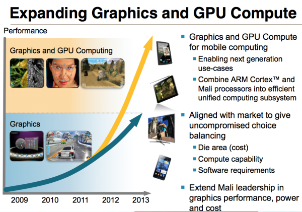
Mobile GPUs aren't immune to making this tradeoff. As mobile devices become the computing platform of choice for many, the same difficult decisions about balancing GPU compute and graphics performance must be made.
ARM announced its strategy to dealing with the graphics/compute split earlier this year. In short, create two separate GPU lines: one in pursuit of great graphics performance, and one optimized for graphics and compute.
Today all of ARM's shipping GPUs fall on the blue, graphics trend line in the image above. The Mali-400 is the well known example, but the forthcoming Mali-450 (8-core Mali-400 with slight improvements to IPC) is also a graphics focused part.
The next-generation ARM GPU architecture, codenamed Midgard but productized as the Mali-T600 series will have members optimized for graphics performance as well as high-end graphics/GPU compute performance.
The split looks like this:

What does the second generation of T600 give you? Higher IPC and higher clock speeds in the same die area thanks to some reworking of the architecture and support for ASTC (an optional OpenGL ES texture compression spec we talked about earlier today).


| |
Read More ...
Anand Chandrasekher Joins Qualcomm

Obviously Qualcomm doesn't need any help getting its SoCs and baseband chips into smartphones and tablets, but what it does need is guidance on the marketing side. Intel and NVIDIA are both well known for being very aggressive with their marketing. Qualcomm has been getting better, but I suspect Anand's goal will be to bring the company up to parity with their rivals. With nearly 14 years of experience at Intel, including a few years in marketing roles, Anand should have some good knowledge to share with his Qualcomm brethren.
It's a smart move for Qualcomm. I've known Anand for over a decade and he definitely has the experience to help address one of Qualcomm's weaknesses. Now we just have to wait to see what Eric is going to cook up over there...
| |
Read More ...
Khronos Announces OpenGL ES 3.0, OpenGL 4.3, ASTC Texture Compression, & CLU
As we approach August the technical conference season for graphics is finally reaching its apex. NVIDIA and AMD held their events in May and June respectively, and this week the two of them along with the other major players in the GPU space are coming together for the graphics industry’s marquee event: SIGGRAPH 2012. Overall we’ll see a number of announcements this week, and kicking things off will be the Khronos Group.
The Khronos Group is the industry consortium responsible for OpenGL, OpenCL, WebGL, and other open graphics/multimedia standards and APIs. At SIGGRAPH 2012 they are making several announcements. Chief among these are the release of the OpenGL ES 3.0 specification, the OpenGL 4.3 specification, the Adaptive Scalable Texture Compression Extension, and the CLU utility for OpenCL. We'll be diving into each of these announcements, breaking them down into the major features and how they're going to affect their respective projects.

| |
Read More ...
Available Tags:GeForce , GTX , Zotac, , Gigabyte , Samsung , Intel , SSD , Galaxy , Microsoft , Windows , MacBook , AMD , Radeon , FirePro , AnandTech , ASUS , Motherboards , Android , HP , NVIDIA , Toshiba , NVIDIA , Apple , iOS ,
No comments:
Post a Comment