
LeEco Announces New Le 2, Le 2 Pro, and LeMax 2
But getting to the topic at hand, LeEco has been making a concerted push into the smartphone space. And today they are updating their smartphone lineup with a trio of devices all appropriately suffixed as 2. These are the Le 2, the Le 2 Pro, and the LeMax 2.
| LeEco Le 2, Le 2 Pro & LeMax 2 | |||
| Le 2 | Le 2 Pro | Le Max 2 | |
| SoC | Helio X20 2x A72 @ 2.3GHz 4x A53 @ 2.0GHz 4x A53 @ 1.4GHz Mali T880MP4 @ 780MHz |
Helio X25 2x A72 @ 2.5GHz 4x A53 @ 2.0GHz 4x A53 @ 1.4GHz Mali T880MP4 @ 850MHz |
Snapdragon 820 2x Kryo @ 1.59GHz 2x Kryo @ 2.15GHz Adreno 530 @ 625MHz |
| RAM | 3GB LPDDR3-1866 | 4GB LPDDR3-1866 | 4/6GB LPDDR4-3733 |
| NAND | 32GB eMMC 5.1 NAND | 32/64GB UFS 2.0 | |
| Display | 5.5" 1080p LCD | 5.7” 1440p LCD | |
| Modem | 2G/3G/4G LTE Cat 6 (Integrated MediaTek SoC Modem) |
2G/3G/4G LTE Cat 12 (Integrated Snapdragon X12 Modem) |
|
| Dimensions | 151.1 (h) x 74.2 (w) x 7.5 (d) mm 153g |
156.8 (h) x 77.6 (w) x 7.99 (d) mm 185g |
|
| Camera | Rear Camera 16MP w/ PDAF |
Rear Camera 21MP IMX230 w/ PDAF |
Rear Camera 21MP IMX230 w/ PDAF & OIS |
| Front Facing Camera 8MP 1.4µm pixels |
|||
| Battery | 3000mAh | 3100mAh | |
| Launch OS | Android 6.0 w/ EUI 5.8 | ||
| Connectivity | 802.11a/b/g/n/ac 2.4 & 5GHz BT 4.2, GPS/GNSS USB-C no 3.5mm headphone jack |
||
| SIM Size | NanoSIM + NanoSIM | ||
| Launch MSRP | RMB ¥1099 (USD~170, ~150€) |
RMB ¥1499 (USD~230, ~205€) |
4GB + 32GB RMB ¥2099 (USD~325, ~285€) 6GB + 64GB RMB ¥2499 (USD~385, ~340€) |
Starting at the flagship level, we have the LeMax 2. Based around Qualcomm’s popular Snapdragon 820, the 5.7” phablet’s spec sheet reads very similar to some of the other flagship phones we’ve seen launched this year. LeEco is pairing the 820 with 32 or 64GB of UFS 2.0 NAND, and as a first for any Android smartphone, up to 6GB of LPDDR4 RAM. To have the first 6GB phone show up here is admittedly unexpected, but given the prevalence of 3GB/4GB configurations elsewhere, it was only a matter of time until someone used higher capacity chips to get to 6GB.
Shifting gears, the display for the phone is a 1440p LCD, which will put it in competition with the likes of the Samsung Galaxy Note5 and S7 series, and the LG G5. The display subjectively looked good with high brightness and good viewing angles. Otherwise for image capture purposes, LeEco has outfitted the phone with a 21MP OIS-capable rear camera, utilizing Sony’s IMX230 sensor. As has been the case for a number of phones this generation, there is a sizable camera hump here to house the camera while keeping the rest of the phone relatively thin. Meanwhile front facing camera duties are handled by a 8MP camera with 1.4µm pixel pitch on the sensor.
Rounding out the package, LeEco is equipping the phone with a 3100mAh battery, and while we’re still working to get the precise battery voltage, at typical voltages we’d be looking at around a total capacity of 11.9WHr. Of course you’ll also find a full suite of wireless connectivity options enabled through the Snapdragon 820, including Qualcomm’s integrated X12 LTE modem, and dual-band 802.11a/b/g/n/ac support.
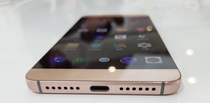
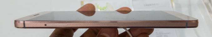
But perhaps the most notable aspect of this phone will be the I/O connectivity. That LeEco is using the increasingly common USB Type-C port is, if anything, to be expected. However what’s unexpected is that this is the only port; a 3.5mm audio jack is not present. Instead the company is piping out audio over the USB port and including a USB Type-C to 3.5mm audio adapter to maintain compatibility with standard headsets. Underlying the USB audio connection in turn is a brand-new technology LeEco is calling CDLA (Continual Digital Lossless Audio).
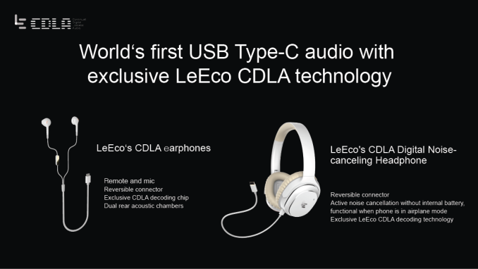
At this point it’s not entirely clear why LeEco went this route; the phone seems to be thick enough to accommodate the 3.5mm jack, so whether this was done for the purposes of giving the space to another feature (e.g. larger speakers) remains to be seen. What the company does claim though is that the audio quality through the CDLA headphones is vastly superior to the 3.5mm analog counterpart, and admittedly at first glance this claim is hard to buy into. I wasn't able to verify this and also unfortunately the devices come with no bundled stock headphones, making this a quite niche accessory.
LeEco will be offering two configurations of the LeMax 2. The 32GB NAND + 4GB RAM configuration will sell for ¥2099, or roughly $325. Otherwise the more spacious 64GB NAND + 6GB RAM configuration will sell for ¥2499 (~$385).
Le 2 (left) vs Le 2 Pro (right)
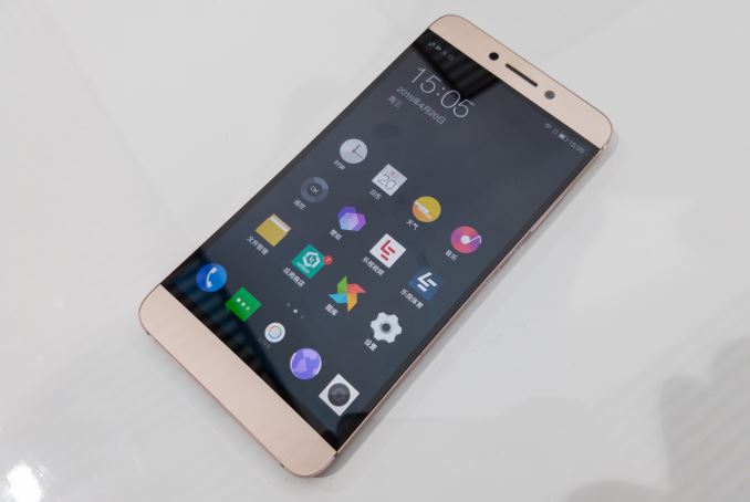
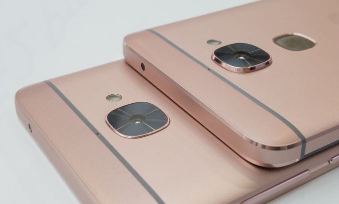
Below the LeMax 2 are the duo of Le 2 series phone, the Le 2 Pro and the simply named Le 2. Both of these phones share the same basic chassis and screen, incorporating a 1080p LCD in a 5.5” phablet form factor. The design is also the same as the LeMax 2 so except for the smaller camera bump on the basic Le 2 you wouldn't be able to tell the difference between the Le 2 Pro and the LeMax 2. The difference, as you might expect from the name, comes from the feature set and price.
Starting with the Le 2 Pro, this phone is based around MediaTek’s Helio X25 SoC, which offers 3 clusters of ARM Cortex CPUs – 2 A53 quad core clusters at different performance/power levels, and a dual core A72 cluster. The X25 in turn is paired with 4GB of LPDDR3 and 32GB of eMMC 5.1 NAND. Also setting it apart from its more basic counterpart is the rear camera module, which like the LeMax 2 is a 21MP camera utilizing Sony’s IMX230 sensor. However OIS doesn't seem to be available in this somewhat smaller phone.
As for the basic Le 2, this sees LeEco dropping down to the lower performance Helio X20 SoC, which cuts down on both the A72 cluster and GPU clockspeeds. The Le 2 gets a smaller 3GB of LPDDR3 RAM and the same 32GB of eMMC 5.1 NAND, however the camera module is a simpler 16MP camera utilizing a hereto-unknown sensor.
Otherwise both phones share identical specifications as far as all other features are concerned. The Helio SoC offers its own integrated Category 6 LTE modem, and both phones incorporate a 8MP front facing camera. And since both phones share the same chassis, both phones also come equipped with a 3000mAh battery. Finally, for I/O and connectivity both phones share the larger LeMax 2’s configuration: dual-band WiFi + Bluetooth 4.2 for wireless data, and the sole USB Type-C port for data and audio.
The Le 2 will be hitting the market at ¥1099 (~$170), while the more powerful Le 2 Pro adds another ¥400 to the price tag, bringing it to ¥1499 (~$230). Today's launch is a China-only launch, however LeEco is pointing out that in the future we'll be seeing focus on the US as its next target market outside of their established market in China and India with the possible introduction of derivative models with modifications to the specifications such as different SoC choices.


Read More ...
Intel Announces Q1 Fiscal Year 2016 Results: Lower Margins Prompt Workforce Adjustments
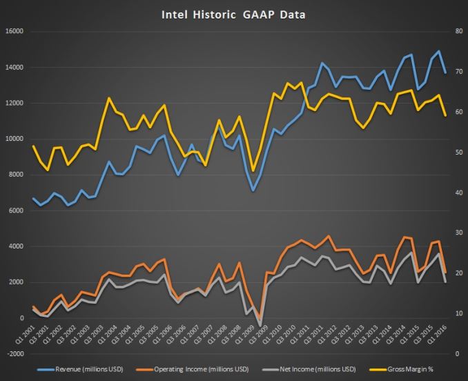
On a GAAP basis, the news is not quite what you would expect for a company that is slashing its operating costs through employee reductions. Revenue for the quarter came in at $13.7 billion, which is up 7% year-over-year. Some of the gain though can be attributed to changes in Intel’s reporting methods, as it has aligned its fiscal year with the calendar year, resulting in an extra week of time for this quarter compared to a typical quarter. Perhaps a more telling result is Intel’s gross margin, which fell to 59.3% for Q1, down 1.2% from last year. Operating income was flat despite the gain in revenue, coming in at $2.6 billion. Net income was up 3% to $2.046 billion, and earnings per share were up 2% to $0.42.
| Intel Q1 2016 Financial Results (GAAP) | |||||
| Q1'2016 | Q4'2015 | Q1'2015 | |||
| Revenue | $13.7B | $14.9B | $12.8B | ||
| Operating Income | $2.6B | $4.3B | $2.6B | ||
| Net Income | $2.0B | $3.6B | $2.0B | ||
| Gross Margin | 59.3% | 64.3% | 60.5% | ||
| Client Computing Group Revenue | $7.5B | -13.8% | +1.74% | ||
| Data Center Group Revenue | $4.0B | -7.17% | +8.64% | ||
| Internet of Things Revenue | $651M | +4.16% | +22.14% | ||
| Non-Volatile Memory Solutions Group | $557M | -14.83% | -5.91% | ||
| Intel Security Group | $537M | +4.88% | +12.11% | ||
| Programmable Solutions Group | $359M | - | - | ||
| All Other Revenue | $50M | -15.25 | -34.21% | ||
Intel also reports Non-GAAP results which exclude certain factors such as acquisition costs, deferred revenue write-downs, inventory valuation adjustments, restructuring charges, and a few other factors. On a Non-GAAP basis, revenue was up 8% to $13.8 billion, gross margin was up 1.3% to 62,7%, operating income was up 13% to $3.3 billion, net income was up 19% to $2.6 billion, and earnings per share came in at $0.54, which is up 20% year-over-year. One of the big factors in the non-GAAP numbers are due to the acquisition of Altera, which was completed early in fiscal year 2016.
The Client Computing group is the largest part of Intel on a revenue basis, and is the one that is feeling the pressure of the declining PC market the most. This segment had $7.5 billion in revenue for the quarter, which is up 2% from the same time last year, but breaking down the numbers we see that there was a decrease in volume of sales of 15%, but the average selling price increase of 19% means there was a small gain year-over-year. Operating income for this segment was $1.9 billion, which is up from the $1.4 billion a year ago. Notebook chips had a flat average selling price, and saw a 2% decrease in volume, while desktop chips sales fell 4% but had a 6% increase in average selling price. Tablet sales saw the biggest hit, down 44% to 4 million units. The tablet market has not matured at the rate initially expected, and Intel has gotten rid of the contra-revenue plan to boost tablet sales, so this is not unexpected. With strong competition from ARM based designs in this segment, Intel is hoping design wins in 2-in-1 devices will help.
The Data Center Group was almost the opposite, with a strong growth in unit sales, up 13% from a year ago, but average selling price fell 3%. Revenue for this group was $4 billion, up from $3.7 billion a year ago, but with the decline in ASP the operating income was only up $65 million to $1.764 billion for the quarter.
Internet of Things posted revenue of $661 million, up from $533 million a year ago. The growth continues in operating income for this new segment of Intel, which saw a 41% gain over last year, and was at $123 million for the quarter.
Intel also has some new reporting segments this quarter. They have added Non-Volatile Memory Solutions, Intel Security Group, and Programmable Solutions Group. The latter is a new segment based on their acquisition of Altera and will be for their expanded FPGA business. The others are branching off from Software and Services and All Other.
Non-Volatile Memory had a drop in revenue of about 6%, to $557 million, and took a $95 million operating loss for the quarter, down from $72 million in operating income last year. The Intel Security Group had revenues up 12% to $537 million, and operating income up to $85 million for the quarter, which is an increase of 286% over the $22 million last year. The Programmable Solutions Group, being a new addition to Intel, only has results from this quarter, which were $359 million in revenue and $200 million in operating loss with the acquisition costs.
Finally, the All Other group had revenue of $50 million, and had an operating loss of $994 million for the quarter. Intel used to have quite a bit of technology under All Other, but with the new reporting groups much of that has been shifted out. It now features operations from the “New Technology Group” as well as restructuring charges, employee benefits, and other expenses.
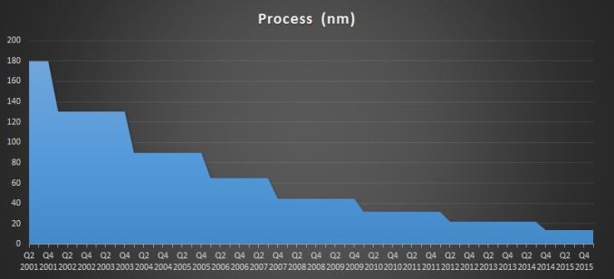
Clearly with the large layoffs announced today, Intel is trying to refocus its efforts on markets where it can continue to grow. Their success in the PC market has been quite pronounced, but with that major market shifting to slower upgrades and fewer unit sales, Intel is going to try again to go after markets where it sees opportunities. One such market was mobile, but Intel was very slow out of the gate to latch on to that, and we are only now seeing Atom parts on a regular update cadence with Goldmont announced for later in the year. Airmont cores never even found their way into a smartphone SoC, meaning that any Intel powered phones were still the older 22nm cores.
It's unlikely anyone but investors like to see companies shed so much of their workforce, and this could be a big impact on Intel in the future with fewer resources to throw at problems, but it could also mean a leaner, more agile company. Time will tell on that story.
Looking at the immediate future, Intel has forecasted revenue of $13.5 billion, plus or minus $500 million for next quarter, which will return to a 13-week quarter as well. Non-GAAP margin is expected to be 61%, plus or minus a couple of percentage points (and yes that’s pretty vague), and with the job cuts they are expecting to take a one time charge of $1.2 billion.
I think Intel has weathered the slowdown in the PC market better than most companies, but they are not immune to the effects, and today we see them trying to offset those losses and move into new markets to win back some of their margin. We’ll keep an eye on their results over the next several quarters and see how they do. They are already getting 40% of their revenue and 60% of their margin from non-PC segments, so they see a good opportunity here to expand that.
Source: Intel Investor Relations
Read More ...
Intel Announces Major Workforce Restructuring: 11% of Workforce to Be Cut Over Next Year
The job cuts themselves are expected to involve up to 12,000 employees, or about 11% of the company’s workforce. Intel will be eliminating positions through a combination of both voluntary and involuntary layoffs, and in the process will be consolidating the remaining workforce and their respective sites. Intel expects the bulk of the layoffs to occur within the next 60 days, with the entire process stretching into mid-2017.
The company’s pre-earnings announcement does not state where these layoffs will come from, and we’re expecting at least some additional detail to come out of the company’s earnings call which is still on-going. However the company is reiterating what markets and businesses they see as growth opportunities and will be investing into for the future, which offers some basic guidance on what the company sees as their most important businesses. Intel’s Data Center and Internet of Things businesses are specifically being cited as their stand-out businesses, which combined with memory and FPGAs provided 40% of the company’s revenue and a majority of their operating profit. Meanwhile in the consumer/client market Intel has seen good returns on 2-in-1s, gaming and home gateways. Conversely, the overall (client) PC market is still in decline, and I expect that a number of the cuts will be centered on that.
Finally, Intel has also detailed the costs of their restructuring. The company will incur a one-time charge of $1.2 billion in Q2, with this presumably being a significant number of severance payments. In turn, the company expects to save $750 million this year, with an annual run rate savings of $1.4 billion per year after the last of the layoffs are completed in mid-2017.
We’ll update this article later today with more information once it comes out of Intel’s earnings call. Ultimately the soft PC market has been a continuing trend for Intel over the past few years, so that we’re seeing Intel react to it now is not unexpected. However it will be important to see just how the layoffs are organized – for example, if Intel makes much in the way of cuts in the fab business – as Intel is a large company. What this means for future client PC investments, mobile, could prove to be significant.
Update: Intel's earnings call has shed a bit more light on the restructuring, but Intel is not spelling out exactly where the bulk of the cuts are coming from at this time.
Overall Intel did reiterate that although the client business has been weak, the company's restructuring plans will be touching more than the client business. The impact to the client business then is that it is being refocused via the restructuring, hence the earlier comments on what Intel sees as the client growth markets. Undoubtedly aspects of the client business are in the crosshairs given the continued slowness in the market, but Intel isn't saying too much more than that.
The company has also made it clear that they're not backing off on fab/manufacturing investments in the near future. Capital expenditures on 10nm and 3D NAND continue untouched even with the restructuring, and overall Intel's technology cadence plans have not changed. Farther ahead, the company has indicated that they are being mindful of their capable competition, and that they need to stay ahead of them, including getting back to a two-year cycle if at all possible.
Finally, Intel has offered a bit more information on the timeline for the restructuring itself. While the majority of the notices to employees will go out in 60 days, the projection is that only about half of the layoffs will be completed by the end of this year, which implies the rest will happen in H1 2017. Part of this comes down to the fact that while Intel has a target number for employment, they have not decided whether they will end any product lines entirely. Intel is in the process of undergoing a complete review of the business to identify any products the company may want to cease, and Brian Krzanich has said that when the review is done there's likely to be a few products that get flagged.
Read More ...
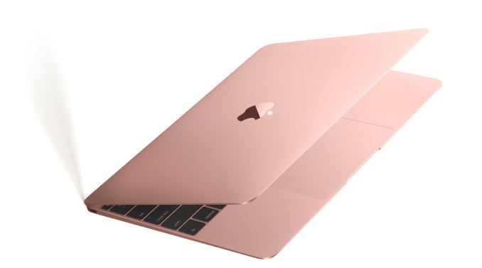
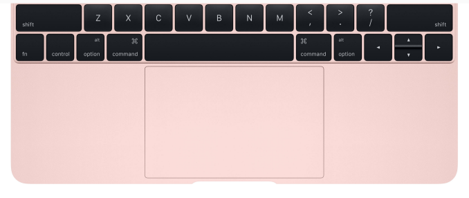
Apple Refreshes MacBook with Skylake-based Core M and New Rose Gold Color
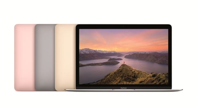
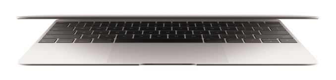
The new Apple MacBook line is based on the dual-core Intel Core M processors based on the newest Skylake microarchitecture as well as the ninth-generation of Intel's integrated graphics (HD 515, Gen9) with improved media playback support. The new processors are the Core m3-6Y30, the Core m5-6Y54 and the Core m7-6Y75, but are upgraded from their listed base frequencies due to Apple using them in a 'configurable 7W TDP up' mode. This adjusts the base frequency up by 100-200 MHz and offers more TDP headroom for longer turbo periods. The latest microarchitecture and increased frequencies should increase the base performance of the new laptops in general-purpose applications whereas hardware-accelerated playback of HEVC and VP9 video streams should improve battery life in video streaming scenarios. Just like predecessors, the new laptops use 8 GB of memory, using LPDDR3 to minimize power consumption of memory sub-system. This time, Apple uses LPDDR3-1866 memory for its MacBook, which is a tad faster than the LPDDR3-1600 DRAM it used last year. This should have a knock-on effect on the integrated graphics performance as well.
| Apple MacBook Line | |||||||
| 2015 (Broadwell) | 2016 (Skylake) | ||||||
| CPU | SKU | Intel Core M-5Y31 |
Intel Core M-5Y51 |
Intel Core M-5Y71 |
Intel Core m3-6Y30 |
Intel Core m5-6Y54 |
Intel Core m7-6Y75 |
| cTDP Up | 7W cTDP Up | ||||||
| Base | 1.1 GHz | 1.2 GHz | 1.3 GHz | 1.1 GHz | 1.2 GHz | 1.3 GHz | |
| Turbo | 2.4 GHz | 2.6 GHz | 2.9 GHz | 2.2 GHz | 2.7 GHz | 3.1 GHz | |
| GPU | SKU | Intel HD Graphics 5300 (GT2) 24 EUs, Gen 8 |
Intel HD Graphics 515 (GT2) 24 EUs, Gen 9 |
||||
| Base | 300 MHz | 300 MHz | |||||
| Turbo | 850 MHz | 900 MHz | 850 MHz | 900 MHz | 950 MHz | ||
| DRAM | 8GB LPDDR3-1600 | 8GB LPDDR3-1866 | |||||
| PCIe SSD | 256 GB | 512 GB | 256 GB 512 GB |
256 GB | 512 GB | 256 GB 512 GB |
|
| PCIe 2.0 x4 | PCIe 3.0 x4? | ||||||
| Display | 12-inch 2304x1440 IPS LCD | ||||||
| Ports | 1 x USB 3.1 (Gen 1) Type-C 3.5mm combo jack |
||||||
| Network | 2x2:2 802.11ac with BT 4.0 | ||||||
| Battery | 39.7 Wh | 41.4 Wh | |||||
| Dimensions | H: 0.14-0.52-inch W: 11.04-inch D: 7.74-inch |
||||||
| Weight | 2.03 lbs (0.92 kg) | ||||||
| Colors | Space Gray Gold Silver |
Space Gray Gold Silver Rose Gold |
|||||
| Price | $1299 | $1599 | $1749 | $1299 | $1599 | $1749 ? | |
Since the chassis and the monitor essentially remained the same as last year, we are still talking about a machine with 12” IPS display panel with 2304x1440 resolution and a full-size keyboard. The maximum thickness of the new MacBook is 1.31 cm (0.52”) and the weight is 0.92 kg (2.03 pounds), similar to the first-gen model.
Apple claims that the new MacBook laptops feature upgraded solid-state storage, which relies on the PCIe bus, but it offers higher performance than the previous-gen SSD the company used on its 2015 MacBook. Last year the company essentially used its own SSD with its own controller, based on iFixit.com’s findings. Perhaps, this year Apple uses a new-gen SSD design developed in-house. Unfortunately, the company remains tight-lipped regarding the nature of its SSD improvements, but only discloses that they are faster than the predecessors. Last year's MacBook used a PCIe 2.0 x4 NVMe interface - moving to Skylake Core M and the fact that Skylake's PCH supports PCIe 3.0 by default means that the new drive is most likely PCIe 3.0, but we're not sure if it is still x4, or if something else has changed. We are asking about this!
In addition to the new components, Apple also uses larger 41.4-watt-hour lithium-polymer terraced battery, compared to a 39.7 watt-hour battery used on the previous-gen model, which should enable longer battery life. Apple itself declares up to 10 hours of wireless web browsing and up to 11 hours of iTunes movie playback, which is an hour longer than before.
The laptop still features a single USB Type-C port with 5 Gbps transfer rate, which can be used for charging, connection to an external display (up to 3840x2160 resolution at 30 Hz refresh rate is supported) and so on. The notebook also has two microphones, a TRRS connector for headsets and a 480p FaceTime camera. Wireless networking capabilities of the notebook also remained untouched: the notebook supports dual-band 2x2 802.11ac Wi-Fi as well as Bluetooth 4.0.
One element worth noting is that the use of Skylake Core M should open up features such as Speed Shift to Apple, where the system has the ability to respond quicker to CPU demands up to 30x and finish quick tasks faster than the previous generation even recognizes the request for a high-performance mode. This becomes significant for responsiveness and user experience, but Speed Shift requires specific OS support. Intel worked closely with Microsoft to enable it for Windows 10, and at this point Apple has not stated publicly if the new MacBook will support Speed Shift out of the box or will be in a future OS update.
The new Apple MacBook laptops are available from Apple directly starting today and from its partners starting April 20, 2016. The most basic Apple MacBook model with Intel Core m3-6Y30 SoC, 8 GB of memory and 256 GB of solid-state storage costs $1299. The more advanced model featuring the Core m5-6Y54 and 512 GB of storage retails for $1599. The Core m7-based model is built-to-order and its price will be higher although we expect it to be similarly priced to the upgraded Broadwell model.


Read More ...
Western Digital Introduces WD Gold HDDs for Datacenters
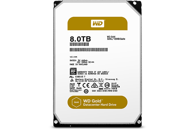
The initial WD Gold family will consist of three models: with 4 TB, 6 TB and 8 TB capacities. All three drives seem to be based on different platforms and on different platters, but all of them have 7200 RPM spindle speed and feature new-generation electronics, which is claimed to improve power efficiency by up to 15% according to WD. The new drives come in a 3.5” form-factor and will use SATA 6 Gbps interface exclusively at this point. The WD Gold HDDs are designed for a variety of applications, including small to medium-scale enterprise servers and storage, as well as rack-mount data center servers and storage enclosures.
| Comparison of Western Digital's WD Gold HDDs | |||||
| WD8002FRYZ | WD6002FRYZ | WD4002FRYZ | |||
| Capacity | 8 TB | 6 TB | 4 TB | ||
| RPM | 7200 RPM | ||||
| Interface | SATA 6 Gbps | ||||
| DRAM Cache | 128 MB | ||||
| NAND Cache | No | Yes | Unknown | ||
| Helium-Filling | Yes | No | |||
| MTBF | 2.5 million | ||||
| Rated Workload (Drive Writes Per Day) | 0.189 | 0.251 | 0.377 | ||
| Equivalent of 550 TB of Writes per Year | |||||
| Acoustics (Seek) | 36 dBA | ||||
| Power Rating | 7.40 W | 9.10 W | |||
| Warranty | 5 Years | ||||
| Price | $629 | $499 | $309 | ||
| $0.0768 per GB | $0.0812 per GB | $0.0754 per GB | |||
| 13.02 GB per $ | 12.31 GB per $ | 13.26 GB per $ | |||
Being data center-oriented HDDs, the WD Gold hard drives are optimized for RAID environments and they support enhanced RAFF technology that protects against vibration (by monitoring linear and rotational vibration in real time) as well as head positioning system with two actuators, which improves positional accuracy. The drives also support WD’s time-limited error recovery technology (TLER), which prevents drive fallout caused by extended HDD error recovery processes.
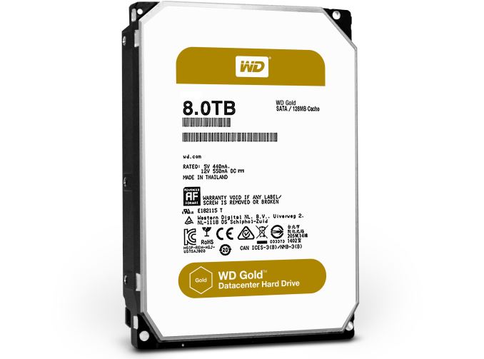
The flagship WD Gold hard drive with 8 TB capacity is Helium based, similar to the HelioSeal platform originally designed by HGST. Western Digital does not reveal the number of platters inside the drive but confirms that these are PMR (perpendicular magnetic recording) platters. Using helium rather than air between the platters helps to reduce power consumption of HDDs compared to non-helium models due to the lower drag force coefficients of helium compared to air - this allows for less friction between heads and the air, as well as platter spinning. All WD Gold HDDs are rated for 2.5 million hours MTBF to signal high reliability.
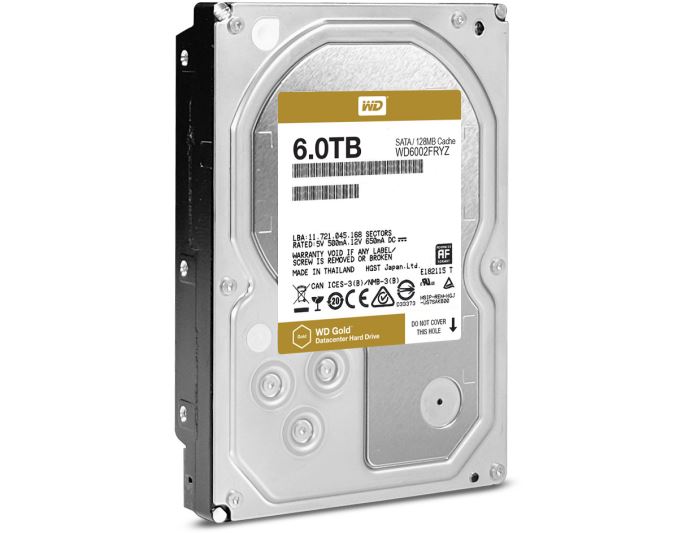
Next up is the WD Gold 6 TB HDD, which uses a more regular HDD arrangement in air, but which features a media-based cache to improve random write performance over the previous generation WD Re 6 TB hard drive. WD is claiming up to 30% better random write performance. Western Digital does not reveal a lot of details about its “media-based cache”, but it is logical to assume that it uses NAND flash memory as a write buffer which then spins down onto the platters during downtime. Unfortunately, we have no idea about its capacity or actual performance. The drive features modern PMR platters and it may be the world’s first data center-class hybrid HDD (with rotating media as well as NAND cache). It is interesting to note that also the drives are sold under the WD trademark, they have HGST's markings, which may mean that they were developed by Western Digital's Japan-based subsidiary.

The entry-level WD Gold 4 TB model is claimed to offer up to 18% sequential performance improvement over previous-generation WD Re 4 TB data center drives, but the company does not reveal whether the new HDDs also feature any media-based cache, or its performance advantages are a result of the new electronics, new platters, and/or a new controller. Just like the 6 TB model, the WD Gold 4 TB has HGST Japan marking.
The new family of WD Gold hard drives demonstrates how Western Digital can build HDDs that are tailored for particular needs, which is becoming more important in an industry that is seeing unit volumes decrease over time. The flagship WD Gold 8 TB is optimized for lower power consumption and higher capacity, whereas the mid-range WD Gold 6 TB is optimized for performance.
The new WD Gold HDDs are available at select distributors and resellers in the U.S. as well as from the company’s online store.
Read More ...
Compulab fitlet-XA10-LAN Review: A Fanless AMD UCFF PC for Networking Applications
Passively cooled computing systems carry many advantages. Most of these turn out to be very important for industrial and embedded applications. The attention paid by AMD and Intel to the peformance per watt aspect of modern day computing platforms has led to ultra-compact form factor (UCFF) PCs emerging as ideal candidates for passive industrial computing platforms. We have already reviewed a number of industrial PCs before. CompuLab is one of the major players in the passively-cooled embedded and industrial computing market space. In this review, we take a look at the CompuLab fitlet-XA10-LAN, a UCFF PC sporting an AMD Mullins SoC along with four gigabit LAN ports.
Read More ...
Intel Unveils New Low-Cost PC Platform: Apollo Lake with 14nm Goldmont Cores

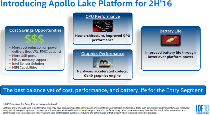
The Apollo Lake system-on-chips for PCs are based on the new Atom-based x86 microarchitecture, named Goldmont, as well as a new graphics core that features Intel’s ninth-generation architecture (Gen9) which is currently used in Skylake processors. Intel claims that due to microarchitectural enhancements the new SoCs will be faster in general-purpose tasks, but at this stage Intel has not quantified the improvements. The new graphics core is listed as being more powerful (most likely due to both better architecture and a higher count of execution units), but will also integrate more codecs, enabling hardware-accelerated playback of 4K video from hardware decoding of HEVC and VP9 codecs. The SoCs will support dual-channel DDR4, DDR3L and LPDDR3/4 memory, which will help PC makers to choose DRAM based on performance and costs. As for storage, the Apollo Lake will support traditional SATA drives, PCIe x4 drives and eMMC 5.0 options to appeal to all types of form-factors. When it comes to I/O, Intel proposes to use USB Type-C along with wireless technologies with Apollo Lake-powered systems.
| Comparison of Intel's Entry-Level PC and Tablet Platforms | ||||||
| Bay Trail | Braswell | Cherry Trail | Apollo Lake | |||
| Microarchitecture | Silvermont | Airmont | Airmont | Goldmont | ||
| SoC Code-Name | Valleyview | Braswell | Cherryview | unknown | ||
| Core Count | Up to 4 | |||||
| Graphics Architecture | Gen 7 | Gen8 | Gen8 | Gen9 | ||
| EU Count | unknown | 16 | 12/16 | unknown (24?) | ||
| Multimedia Codecs | MPEG-2 MPEG-4 AVC VC-1 WMV9 HEVC (software only) VP9 (software only) |
MPEG-2 MPEG-4 AVC VC-1 WMV9 HEVC (8-bit software/hybrid) VP9 (software/hybrid) |
MPEG-2 MPEG-4 AVC VC-1 WMV9 HEVC VP9 |
|||
| Process Technology | 22 nm | 14 nm | 14 nm | 14 nm | ||
| Launch | Q1 2014 | H1 2015 | 2015 | H2 2016 | ||
From the IDF presentation, Intel shares only a few brief details regarding its new Apollo Lake design platform, but does not disclose exact specifications or performance numbers. At this point, based on 14nm Airmont designs, it is pretty safe to assume that the new SoCs will contain up to four Goldmont cores in consumer devices but perhaps 8+ in communications and embedded systems. Intel has not specified the TDP of its new processors but claims that power management features of the platform will help it to improve battery life compared to previous-gen systems (which might point to a Speed Shift like arrangement similar to what we see on Skylake, perhaps). While Intel does not reveal specifics of its own SoCs, the company shares its vision for the upcoming PCs powered by the Apollo Lake platform.
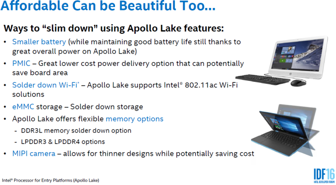
Firstly, Intel believes that the upcoming affordable PCs, whether these are all-in-one desktops, miniature systems, 2-in-1 hybrids, laptops or tablets, should be very thin. According to their market research, this will make the devices more attractive to the buyer, which is important. To make systems thinner, Intel traditionally proposes to use either M.2 or solder-down eMMC solid-state storage options instead of 2.5” HDDs/SSDs. In addition, the company believes that it makes sense to use solder-down Wi-Fi, instead of using a separate module. Intel seems to be especially proud with the compactness of the Apollo Lake SoC (as well as other core components) and thus the whole platform, which is another factor that will help to make upcoming systems thinner. For the first time in recent years, Intel also proposes the use of smaller batteries, but devices can maintain long battery life by cutting the power consumption of the entire platform. While in many cases reduction of battery size makes sense, it should be noted that high-resolution displays typically consume a lot of energy, which is why it is hard to reduce the size of batteries, but maintain the visual experience along with a long battery life.

Secondly, PCs based on the Apollo Lake should be very affordable, which is why Intel’s reference core components design can be used for different form-factors (AiO and mobile). Additionally, the company reveals a number of BOM (bill of materials) savings opportunities, which are a result of higher level of SoC integration as well as a recommended choice of components. In the slide above, using all the savings can make a difference in BOM for between $5.55 and $7.35, which could mean double memory or a better display for the same price for the new generation.

Intel’s reference design for Apollo Lake-based PCs seems to be a tablet/2-in-1 hybrid system with an 11.6” full-HD (1920x1080) 10-point multi-touch display, 4 GB of LPDDR3-1866 memory, 64 GB M.2 SATA3 SSD or 32 GB eMMC storage, an M.2 wireless module supporting 802.11ac, an optional M.2 LTE modem, an integrated USB 2 camera, a host of sensors (accelerometer, ambient light, proximity detection, and magnetic switching) as well as a USB Type-C connector supporting USB power delivery and alternate modes. Such reference design can power not only mobile, but also Aan IO and even small form-factor desktop PCs. Still, given the fact that we are talking about low-cost systems, do not expect retail computers to feature multiple storage devices and LTE modems. However, PC makers may opt for more advanced displays as well as better integrated cameras, or an SI might plump for a half-price 'Macbook-like' device design using Type-C, albeit on the Atom microarchitecture. This is Intel's vision forthe next generation of Chromebooks: the 'cloud book' market.

PCs based on Intel’s Apollo Lake platforms will emerge in the second half of the year and will carry Celeron and Pentium-branded processors. At present, entry-level notebooks (which Intel calls Cloudbooks) offer 2 GB of memory, 32 GB of storage, 8+ hours of battery life and ~18mm thick designs. With Apollo Lake, OEMs should be able to increase the amount of RAM and/or storage capacity, make systems generally thinner, but maintain their $169 - $269 price-points. Intel also believes that its Apollo Lake presents great opportunities to build 2-in-1 hybrid PCs (convertibles) and capitalize on higher margins of such systems.

Traditionally, Intel discusses options and its vision, but not actual PCs, at its IDF trade-shows. It remains to be seen whether PC makers decide to build low-cost convertibles or ultra-thin notebook designs, or will stick to more traditional clamshell notebooks. In fact, we will learn more about BTS (back-to-school) plans of major PC OEMs regarding Apollo Lake at the upcoming Computex trade-show in early June. There's also IDF San Francisco in August where Intel may open some lids on how the new Goldmont core differs from Airmont.


Read More ...
OpenPOWER Gains Support as Inventec, Inspur, Supermicro Develop POWER8-Based Servers
IBM to Expand Power Systems: LC Server Family with Support from Supermicro
Last week IBM disclosed plans to expand the lineup of its Power LC servers that are based on the POWER8 microprocessors as well as Linux operating system. In particular, the company intends to add Open Compute Project-compliant systems for big data analytics to the Power Systems LC portfolio, which will be important for the company as well as Open Compute Project in general. In addition, Supermicro will develop two servers that will be sold under IBM’s Power LC brand.
Supermicro is currently working on a 2-way IBM POWER8-based 2U server with up to 512 GB of DDR4 memory, 12 LFF/SFF hot-swap drive bays, and either two NVIDIA Tesla K80 or two Alpha-Data KU3 CAPI adapters (based on the Xilinx UltraScale KU115 FPGA). Another machine that Supermicro is working on is a 1U server featuring two IBM POWER8 processors, 512 GB of DDR4 memory, and either one NVIDIA Tesla K80 or two Alpha-Data KU3 CAPI adapters, as well as four hot-swap drive bays. The servers feature Supermicro’s “Ultra” architecture, which enables the company to maximize density of devices inside its chassis, which means greater expansion capabilities and flexibility for the platform.
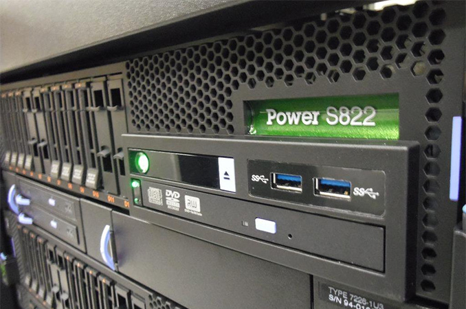
Right now, IBM sells the Power S812LC (1-way system with up to 10 cores, up to 1 TB of memory and up to 14 storage devices in 1U form-factor) and the Power S822LC (2-way system with up to 20 cores, up to 1 TB of memory, two NVIDIA Tesla K80 accelerators in 2U form-factor) developed by Tyan and Wistron, respectively. Adding Supermicro, one of the world’s largest producers of x86 servers, to the list of POWER8 suppliers is an important step for IBM. Still, at present, it does not look like Supermicro plans to sell POWER8-based servers under its own brand directly.
POWER8-Based Machines from Inventec and Wistron Incoming
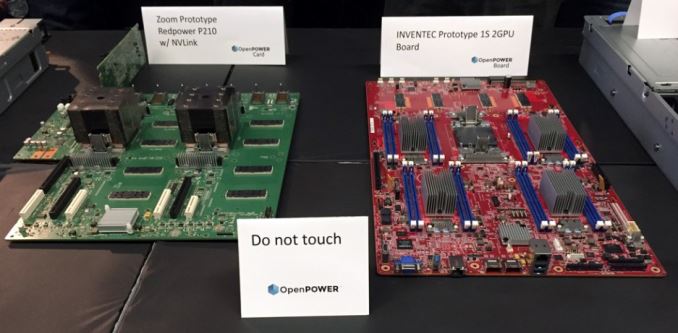
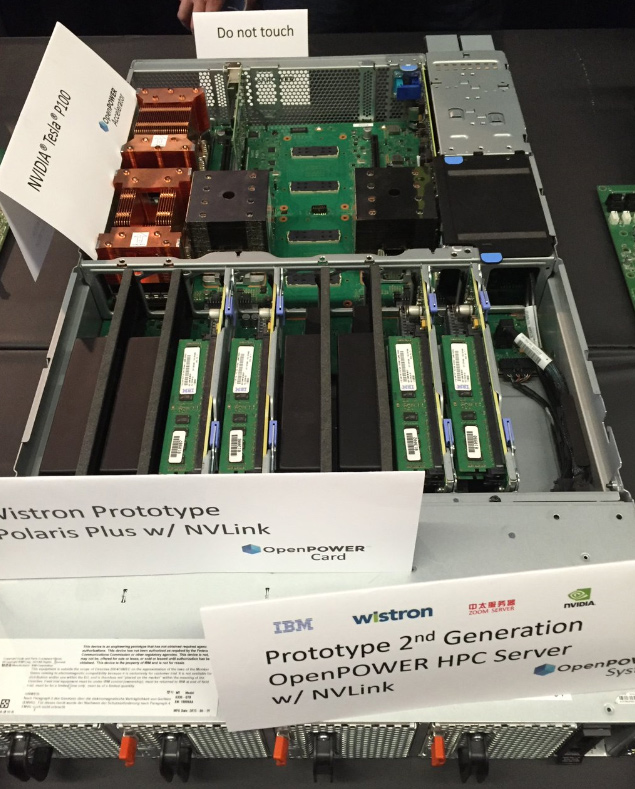
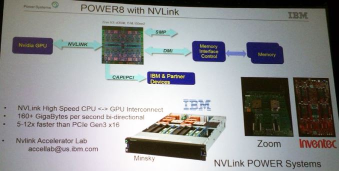
Supermicro is not the only big server maker to develop POWER8-based machines. Inventec, a major Taiwan-based ODM that sells, inter alia, servers to such companies as Dell and Lenovo, is also working on an OpenPOWER project. The platform will be based on one IBM POWER8 CPU with NV-Link as well as two NVIDIA Tesla P100 compute accelerators. The machine will also feature 16 DDR4 DIMMs (thanks to IBM’s Centaur memory buffer chip) and will thus support a lot of memory (at least, for a 1-way system). Inventec’s POWER8-based platform is designed primarily for high-performance computing (HPC) and it remains to be seen in what form it will actually reach the market (and whether it will reach it at all). Right now, this is only a motherboard project, therefore, it could be a prototype for evaluation by customers, or a prototype for an undisclosed interested party (which is also interesting, given Inventec’s list of customers).
Wistron, which is another major Taiwan-based server ODM, is working with NVIDIA, IBM and Mellanox on a prototype of a 2-way IBM POWER8-based machine with four Tesla P100 accelerators aimed at HPC applications which we told you about last week. However, the company is developing three more OpenPOWER products. The first product, available today, is Wistron Polaris (co-developed with E4 Computer Engineering), a 2-way 2U system featuring IBM POWER8 CPUs with CAPI support. The Polaris is aimed primarily at HPC applications. Later on, Wistron plans to offer its Polaris Plus, which will resemble the machine co-developed with IBM and NVIDIA: it will feature two POWER8 processors with NVLink as well as four NVIDIA Tesla accelerators featuring Pascal architecture. Finally, the company is working on the Dark King project, a 4-way 4U server with POWER8 CPUs, 128 DIMMs (and several terabytes of memory) and CAPI support. The Dark King will be designed for large-scale data analysis.
Speaking of E4, it naturally offers what it co-developed with Wistron: the E5 OP205 2-way 2U server with support for CAPI accelerators for various industries that require high-performance computing.
POWER Gains Support from Chinese Server Makers
Another noteworthy company, which is designing two POWER8-based servers, is China-based Inspur. Inspur is among the largest makers of servers in the country. The manufacturer is working on 1-way and 2-way 4U machines for new data center and big data applications. Not a lot of information is known about Inspur’s 2-way IBM POWER8 4U server, except the fact that it will support up to 2 TB of DDR3 memory (using 64 DIMMs).
Undisclosed partners from OpenPOWER Foundation also helped Beijing Neu Cloud Oriental System Technology to develop the NL2200 2-way server that supports IBM POWER8 chips with up to 12 cores, up to 1 TB of memory, two GPU-based compute accelerators, two hard drives, a PCIe-based SSD as well as a 100 Gbps Infiniband adapter. Such machine could be used for HPC and other applications and its development just shows that some China-based companies are investing into OpenPOWER.
One more Chinese server maker, which demonstrated its products at OpenPOWER’s Summit last week, was Zoom Server. They showcased their Redpower C210/C220 and P210 machines. The C210/C220 is a 2-way system with up to 12 storage devices, which is aimed at data storage, database and other applications. Meanwhile, the P210 by contrast is a more advanced server for HPC, which is powered by two IBM Power8+ CPUs that support four NVIDIA Tesla compute processors with NVLink (e.g., Tesla P100) and up to 1 TB of memory.
While three server makers from China is not a lot, keep in mind that OpenPOWER Foundation is only several years old and the vast majority of datacenter owners are not familiar with IBM’s POWER8 processors. Therefore, the fact that Inspur and smaller companies are building POWER8-based systems could show potential and viable performance offered by such servers, but not that they are gaining market share just yet.
Availability of Open Compute Project-Compliant Servers to Expand
In addition to custom systems from large server manufacturers, a number of companies (including Mark III Systems, Penguin Computing and Stack Velocity) are also offering/working on Open Compute Project-compliant OpenPOWER systems. Such machines are important because server makers will sell them to software developers, who would like to optimize their programs for IBM’s POWER8, as well as to companies who would like to try POWER-based systems. In the long term, this could help increase market share of IBM’s POWER8 platforms in datacenters.
For example, Penguin Computing offers the Magna 2001 for software development, the Magna 1015 (1-way IBM POWER8) for Open Rack infrastructure and virtualization workloads as well as the Magna 2002 (2-way IBM POWER8, NVIDIA Tesla K80 or M40 accelerator) for accelerated computing and machine learning applications. Mark III Systems will offer IBM POWER8-based servers which will rely on the Open Compute Project design specification and will follow the Barreleye server design by Rackspace (2-way IBM POWER8, 32 DIMMs, CAPI, etc.). Meanwhile, StackVelocity intends to sell a machine based on the Barreleye server design as well as Saba 2U system with POWER8 and CAPI accelerators for big data analytics and HPC applications.
POWER9-Based Systems in Development
It is also noteworthy that Google and Rackspace are already working on server architecture specification based on the upcoming IBM POWER9 microprocessors, which may indicate that the two companies are interested in the chip as well as the next-gen POWER servers.
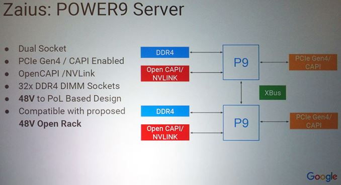
This custom server plan developed by Google and Rackspace is code-named Zaius. The machine will not come online until the POWER9 CPUs are officially released by IBM in the roadmaps, but Google is already sharing some of its details. The Zaius will be based on two IBM POWER9 processors (with an unknown amount of cores) and will feature 32 DDR4 DIMM slots (which helps to double the amount of memory vs. Barreley). The POWER9 processors will support both NVLink and CAPI, therefore, the Zaius will be compatible not only with FPGA-based accelerators but also with NVIDIA’s Tesla P100 and other upcoming GPU-based compute solutions from the company. Such compatibility will let Google and Rackspace deploy NVIDIA’s Tesla processors more broadly than today. What is important is that the POWER9 are also expected to bring support for PCIe 4.0 next year, which means higher bandwidth for storage and various accelerators.
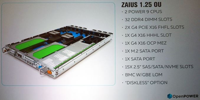
The Zaius server will be compatible with proposed Open Rack 48V and will be 1.25U in height. It will be able to house two full-length full-height PCIe 4.0 x16 cards, one half-length half-height PCIe 4.0 x16 card, one device connected using a mezzanine PCIe 4.0 x16-based OCP connector as well as up to 15 2.5” SAS/SATA/NVME storage devices.
According to Google, many of its cloud services, including Gmail, are already processed by systems featuring IBM’s Power8 processors. Apparently, the company finds performance of these CPUs competitive and IBM’s microprocessor roadmap promising, which is why it is co-developing POWER9-based server with Rackspace.
A long-term commitment from companies like Google and Rackspace is not something to underestimate. It shows that two major users of servers plan to continue adopting IBM POWER-supporting software and hardware, thus, helping to create an alternative for Intel’s Xeon platform (which is important for the market in general).
Sources: OpenPOWER Foundation, Nikkei IT Pro.
Image Sources: IBM Power Systems Japan, Rackpace, Nikkei IT Pro.
Read More ...
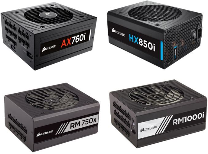
Corsair Extends Warranty of Advanced PSUs to 10 Years
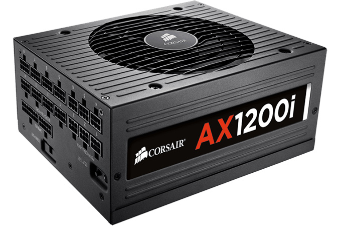
Effective immediately and retroactively, Corsair has increased the warranty of all AXi range (launched in 2012), HXi range (launched in 2014) and RMi/RMx range (launched in 2015) PSUs from 7 years to 10 years. The extended warranty covers not only newly purchased power supplies, but also all the PSUs that belong to the aforementioned families sold to date.
Note that Corsair did not extend warranties on its regular AX, HX and RM/RX PSUs, which were on the market for a long time, but now are not available from the company. While those power supplies are considered as good, Corsair upgraded capacitors, fans, heatsinks and some other internal components in their new PSU lineups (see our review of the RM1000i and the RM1000x PSUs for details), not to mention changed OEMs in some cases.
Most of power supplies on the market today are covered by 3 or 5 year warranties, but Antec, Seasonic and Thermaltake offer 7 year warranties on high-end PSUs. To date, only EVGA has covered its select PSUs with a 10 year warranty. As it appears, Corsair’s AXi, HXi, RMi and RMx power supplies are so good that Corsair wants to extend their warranties in a bid to show that.
Owners of Corsair’s power supplies do not need to register or contact the manufacturer anyhow to get the extra warranty coverage.
Source: Corsair (via The Tech Report)
Read More ...
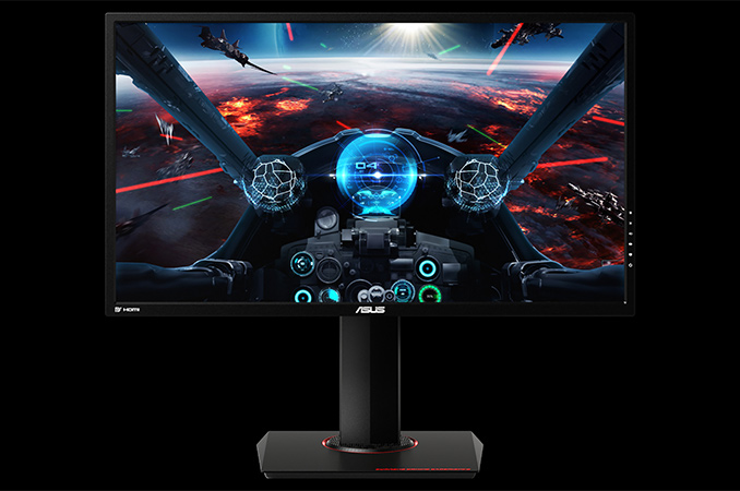
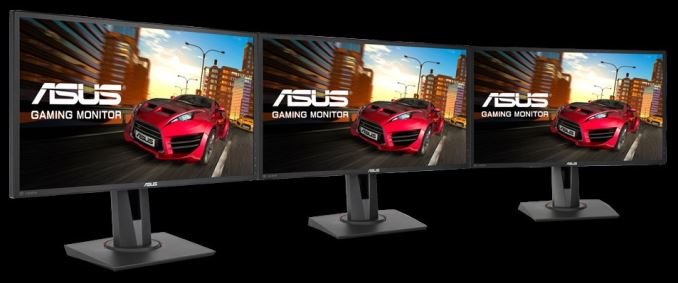
ASUS Announces Three New Displays with Adaptive-Sync Technology
| Specifications of ASUS MG-Series Displays | |||||
| MG248Q | MG24UQ | MG28UQ | |||
| Panel | 24" TN | 23.6 IPS | 28" TN | ||
| Resolution | 1920 x 1080 | 3840 x 2160 | |||
| Refresh Rate | 40 Hz - 144 Hz | 30 Hz - 60 Hz | |||
| Adaptive-Sync Range |
unknown | 40 Hz - 60 Hz | |||
| Response Time | 1 ms gray-to-gray | 4 ms gray-to-gray | 1 ms gray-to-gray | ||
| Brightness | 350 cd/m² | 300 cd/m² | 330 cd/m² | ||
| Contrast | True contrast ratio unknown | ||||
| Viewing Angles | 170°/160° horizontal/vertical | 178°/178° horizontal/vertical | 170°/160° horizontal/vertical | ||
| PPI | 92 ppi | 186 ppi | 157 ppi | ||
| Pixel Pitch | 0.276 mm | 0.136 mm | 0.16 mm | ||
| Colors | 16.7 million | 1.07 billion | |||
| Color Saturation | Unknown | ||||
| Inputs | DisplayPort 1.2 HDMI 1.4 DVI-D |
DisplayPort 1.2 HDMI 2.0 HDMI 1.4 x 2 |
|||
| Audio | 2 x 2 W | ||||
The biggest display among the novelties is the ASUS MG28UQ, which is based on a TN panel with 3840×2160 resolution, and a 330 nit max brightness. The MG28UQ has default refresh rate of 60 Hz and supports dynamic refresh rates between 40 and 60 Hz, which is typical for 4K monitors. The display is equipped with one DisplayPort 1.2 and three HDMI inputs, a dual-port USB 3.0 hub with quick charge support as well as two 2 W speakers. The unit also features tilt, swivel, pivot and height adjustment and is compatible with VESA display wall mounts.
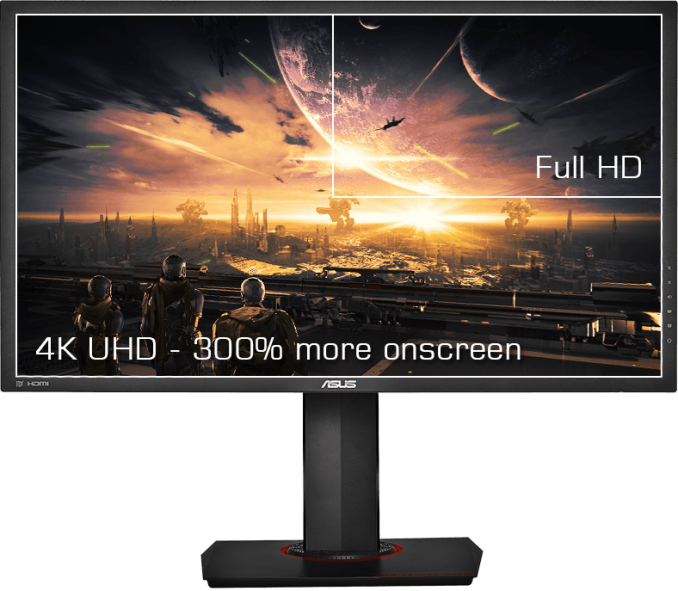
The ASUS MG28UQ is available now for $549 from Amazon. The product does not seem to be very affordable for a TN-based display, possibly because ASUS charges premium for the Adaptive-Sync feature. Nonetheless, the monitor is not too expensive either.
Next up, the MG24UQ is not as big as its large brother (it has 23.6” diagonal), but it will be a more interesting option for those, who prefer IPS panels with high pixel density. The monitor sports 3840×2160 resolution with up to 60 Hz refresh rate and a peak brightness of 300 nits. Adaptive-Sync works for refresh rates between 40 and 60 Hz, just like in case of the MG28UQ. The monitor features one DisplayPort 1.2, three HDMI inputs as well as two 2 W speakers. The design of the MG24UQ display is very similar to that of the MG28UQ (hence, it sports the same set of adjustments and VESA mounts) with the exception of dimensions and the lack of a USB hub on the smaller one.
The ASUS MG24UQ can be pre-ordered now for $399 on Amazon.
Finally, the ASUS MG248UQ is designed for gamers who value high dynamic refresh rates most of all other features. This display will be the first 24” monitor from the company which supports up to 144 Hz refresh rate as well as Active-Sync technology. The monitor uses a TN panel with 1920×1080 resolution and a peak brightness of 350 nits, offering slightly better specifications and a more aggressive visual design compared to the VG247H and the VG248QE. The display supports dynamic refresh rates between 40 and 144 Hz, according to ASUS, which is a very decent range. As an added bonus, thanks to the extremely high refresh rate, the MG248UQ could be used with NVIDIA's 3D Vision stereo-3D kit
ASUS plans to start selling the MG248UQ in the coming weeks for an undisclosed price. Typically, such monitors are not expensive, thus, the MG248UQ could be used to build relatively affordable ultra-fast multi-monitor setups with Adaptive-Sync.
ASUS is one of the leading suppliers of displays for gamers with a huge market share, according to the company. The new MG-series monitors should help ASUS to better address the segment of affordable displays for gamers.


Read More ...
The PNY CS1311 and CS2211 SSD Review: MLC vs TLC at 15nm
PNY's latest consumer SSDs incorporate Toshiba 15nm NAND and are based on the Phison S10 controller. The TLC-based PNY CS1211 and MLC-based PNY CS2211 offer the rare opportunity of a direct comparison of MLC against TLC on the same hardware platform. In addition, they are also reasonably priced for the entry-level and mainstream segments of the SSD market.
Read More ...
AMD Announces 32GB FirePro W9100 - Pro Graphics Gets a Memory Bump
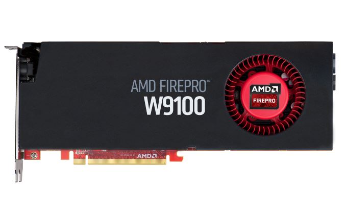
Due to various technical considerations – primarily a larger memory bus – over the past generation AMD has traditionally offered the highest capacity professional graphics cards, with the current FirePro W9100 topping out at 16GB. More recently, last month NVIDIA surpassed AMD with the launch of the 24GB Quadro M6000. However this week in advance of the 2016 NAB Show, AMD is firing back and retaking the top spot with their own capacity bump, updating the FirePro W9100 to 32GB.
| AMD FirePro W Series Specification Comparison | ||||||
| AMD FirePro W9100 (32GB) | AMD FirePro W9100 (16GB) | AMD FirePro W9000 | AMD FirePro W8100 | |||
| Stream Processors | 2816 | 2816 | 2048 | 2560 | ||
| Texture Units | 176 | 176 | 128 | 160 | ||
| ROPs | 64 | 64 | 32 | 64 | ||
| Core Clock | 930MHz | 930MHz | 975MHz | 824MHz | ||
| Memory Clock | 5Gbps GDDR5 | 5Gbps GDDR5 | 5.5Gbps GDDR5 | 5Gbps GDDR5 | ||
| Memory Bus Width | 512-bit | 512-bit | 384-bit | 512-bit | ||
| VRAM | 32GB | 16GB | 6GB | 8GB | ||
| Double Precision | 1/2 | 1/2 | 1/4 | 1/2 | ||
| Transistor Count | 6.2B | 6.2B | 4.31B | 6.2B | ||
| TDP | 275W | 275W | 274W | 220W | ||
| Manufacturing Process | TSMC 28nm | TSMC 28nm | TSMC 28nm | TSMC 28nm | ||
| Architecture | GCN 1.1 | GCN 1.1 | GCN 1.0 | GCN 1.1 | ||
| Warranty | 3-Year | 3-Year | 3-Year | 3-Year | ||
| Launch Price (List) | $4999 | $3999 | $3999 | $2499 | ||
| Launch Date | Q2 2016 | April 2014 | August 2012 | July 2014 | ||
The updated FirePro W9100 takes off right where the previous model left off. Based around a fully enabled version of AMD’s Hawaii GPU, the specifications outside of memory capacity are unchanged. As for the memory itself, this update sees AMD replace their 4Gb GDDR5 chips with 8Gb chips, moving from a 32 x 4Gb configuration to a 32 x 8Gb configuration. Consequently any possible performance impact is data set size dependent. Performance essentially doesn’t change for data sets that fit within memory, while sets between 16GB and 32GB that were slow before because they didn’t fit on the card will now be able to be loaded in their entirety.
With their latest capacity bump, AMD becomes the first company to ship a 32GB pro graphics card, and consequently retakes their top spot in the market. At the same time AMD will have final bragging rights for this generation, as AMD and NVIDIA have now both maxed out the memory capacity of their current cards.
The 32GB FirePro W9100 will be launching this quarter through AMD’s usual distribution and OEM partners. The MSRP will be $4999, which is closely aligned to competitor NVIDIA’s own pricing, though also higher than the 16GB card it supplants. Meanwhile AMD will continue to ship the 16GB card as well, and while there isn’t a current MSRP attached to it, it’s currently available from retailers for around $3000.
Read More ...
GIGABYTE Adds 75W GeForce GTX 950 to Lineup
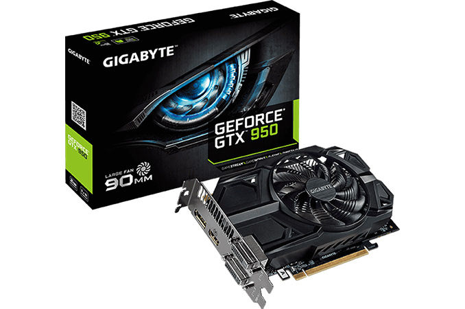
The GIGABYTE GV-N950D5-2GD graphics card is based on the GeForce GTX 950 GPU in default configuration (768 stream processors, 48 texture units, 32 ROPs, 128-bit GDDR5 memory interface), but does not require external power, unlike Nvidia’s reference design of the product. Power consumption of the GV-N950D5-2GD does not exceed 75 W, which is why it can be powered by the PCIe x16 slot. Due to reduced power consumption, the new graphics card from GIGABYTE does not feature significant factory-overclocking, it comes with GPU frequencies of 1051/1228 MHz (base/boost) and thus offers performance close to that of Nvidia’s reference card.

The board is equipped with 2 GB of GDDR5 memory, two DVI connectors, one HDMI 2.0 port and one DisplayPort output. The product uses a rather simplistic dual-slot cooling system with one fan, which should be sufficient given low-power nature of the device. In a bid to ensure long lifespan of the product, GIGABYTE uses high-quality components, such as solid-state inductors and capacitors, to build the GV-N950D5-2GD.
GIGABYTE added its low-power GV-N950D5-2GD graphics card to its lineup after ASUS, EVGA and MSI quietly introduced their GeForce GTX 950-based products with 75 W power consumption that do not require auxiliary six-pin PCIe power connectors. Such adapters can be used to upgrade inexpensive PCs that do not have an extra power connector inside, or to build low-power gaming or HTPC systems. Since the GM206 GPU is still the only GPU on the market that supports hardware-accelerated decoding and encoding of H.265 (HEVC) video, as well as HDCP 2.2 content protection over HDMI 2.0 (which is required for Ultra HD Blu-ray playback), those who build modern HTPCs, do not have a lot of choice.
| NVIDIA GeForce GTX 950 Graphics Cards Specification Comparison | ||||||||
| GIGABYTE GTX 950 |
EVGA GTX 950 | EVGA GTX 950 | MSI GTX 950 |
ASUS GTX 950 |
Ref | |||
| Product Name | GV-N950D5- 2GD |
02G-P4- 0954 |
02G-P5-258 | 2GD5 OCV2 | GTX950-2G | - | ||
| CUDA Cores | 768 | |||||||
| Texture Units | 48 | |||||||
| ROPs | 32 | |||||||
| Core Clock | 1051 MHz |
1025 MHz |
1076 MHz |
1076 MHz |
1026 MHz |
1024 MHz |
||
| Boost Clock | 1228 MHz |
1190 MHz |
1253 MHz |
1253 MHz |
1190 MHz |
1188 MHz |
||
| Memory Clock | 6.6 Gbps GDDR5 |
|||||||
| Memory Bus Width | 128-bit | |||||||
| VRAM | 2 GB | |||||||
| TDP | 75 W | 90 W | ||||||
| Outputs | DVI-D DVI-I DP 1.2 HDMI 2.0 |
DVI-D DVI-I DP 1.2 HDMI 2.0 |
DVI-D DVI-I DP 1.2 HDMI 2.0 |
DVI-I DisplayPort 1.2 HDMI 2.0 |
||||
| Architecture | Maxwell 2 | |||||||
| GPU | GM206 | |||||||
| Transistor Count | 2.94 B | |||||||
| Manufacturing Process | TSMC 28nm | |||||||
| Launch Date | Apr '16 | Mar '16 | Aug '15 | |||||
| Launch Price | unknown | $159 | ||||||
With GIGABYTE’s addition of a GM206-251-based graphics board to its product family, low-power GeForce GTX 950 is now available from virtually all well-known suppliers of video cards. Pricing of GIGABYTE’s GV-N950D5-2GD video card is unknown, but GeForce GTX 950-based adapters are generally inexpensive.


Read More ...
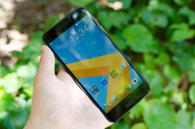
HTC 10: A Quick Look At Battery Life & Storage Performance
As mentioned in part 1 of the Galaxy S7 review, our new web browsing battery life test attempts to have much more realistic workloads. In addition to updating the test pages to modern websites, we’ve added a component of scrolling through webpages which will help with making a more realistic and reasonable test. While we don’t have a touchscreen CPU boost interrupt firing upon scrolling, scrolling introduces a workload that can test how well the governor can select a proper CPU frequency to complete a fixed amount of work over a given amount of time rather than simply detecting a high CPU load and sending the CPU into a maximum performance state. The scrolling component also means that we no longer give PSR more credit than it realistically should have, and provides some kind of stress upon the display pipeline that we previously left unexplored.
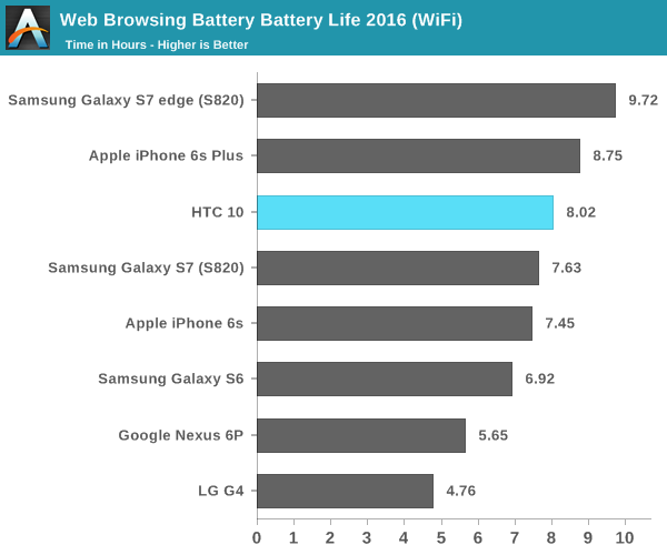
In WiFi, we can pretty clearly see that the HTC 10 actually has a notable lead over the Galaxy S7 with Snapdragon 820, although the difference isn’t necessarily enormous. I’m actually pretty surprised by this showing from the HTC 10 because our test is specifically designed to decrease the average APL with a few pages that have dark themes. Another factor that tilts the scales against the HTC 10 when comparing against phones like the Galaxy S7 is that the Galaxy S7 has an undefeatable power save mode which drops brightness by more than half and throttles the CPU noticeably, while the HTC 10 was run with all power save options disabled.
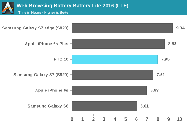
On the LTE side, we see the same sort of pattern continue. Qualcomm’s modem prowress is showing here on the S820 devices, as they’ve managed to get WiFi and LTE power drain to be effectively equal in situations where the power amplifier on the transmit side isn’t trying to pull a watt or so to keep a connection to an eNodeB. Interestingly enough, one thing that our old web browsing test didn’t catch was that LTE modem efficiency on the Galaxy S6 is pretty disappointing. Our new test simulates the effects of ads on webpage loads, so I suspect that the Verizon Galaxy S6’s modem is not very efficient at idle, while the sort of race to sleep workload that we saw in the old web browsing test wouldn’t show these issues.
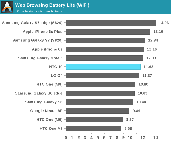
In the interest of having a comparison that is basically almost all static display at this point, I also ran our last generation web browsing test. As another data point it’s pretty interesting because this actually suggests that Samsung AMOLED is more efficient than HTC’s LCD, which is probably a function of the much higher subpixel density as HTC is using RGB stripe instead of PenTile. Given that the HTC 10’s Tianma display definitely doesn’t use photoalignment to achieve higher contrast ratios and its relatively low maximum brightness compared to the Galaxy S7, this result is really more in line with what I was expecting. I’m honestly curious as to what optimizations HTC is doing here to pull off better power efficiency here in our 2016 web browsing test, because the SoC bin in the HTC 10 review unit is noticeably worse than the Galaxy S7 and Galaxy S7 edge that I received. It's unlikely that this will be the case on average when comparing devices as a whole, but for our review it will affect relative results. On top of this, the display doesn’t seem to be particularly efficient compared to the Galaxy S7’s AMOLED display as seen in the test results above.
In the interest of discussing throttling performance and to get an idea for what the lower bound of battery life is like on the HTC 10, I also went ahead and put it through our Basemark OS II and GFXBench battery life test. While we’re actively transitioning to GFXBench 4 and also moving to a newer Manhattan 3.1 battery life test, for 1440p Snapdragon 820 devices our traditional T-Rex rundown is sufficient to show throttling behavior and give an idea of what the lower bound for performance looks like.
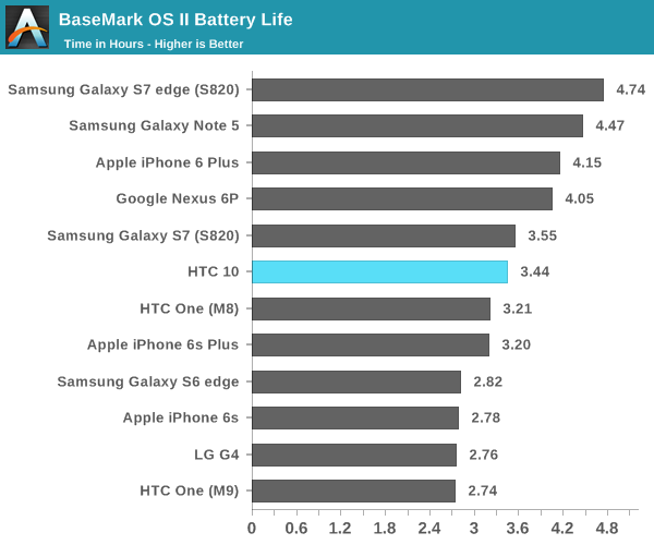
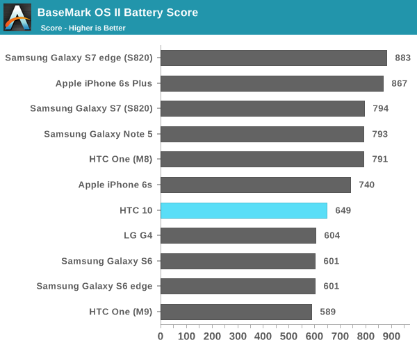
Starting with Basemark OS II, we’re really seeing the effects that a worse bin has on the HTC 10 as the device noticeably trails the Galaxy S7 here, but overall runtime is pretty similar as the difference in display efficiency is going to be minimized. We’re also seeing a difference in the kind of load that the two devices can sustain, as the HTC 10’s aluminum unibody means the maximum allowed skin temperature is going to be lower than what the glass-backed Galaxy S7 will allow. Whatever the case, the Galaxy S7 is ahead here.
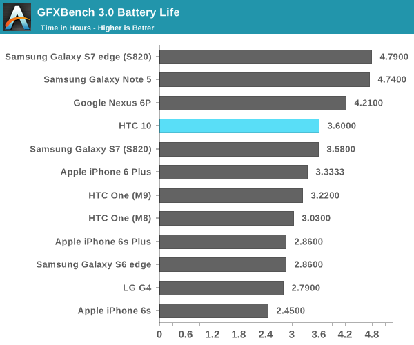
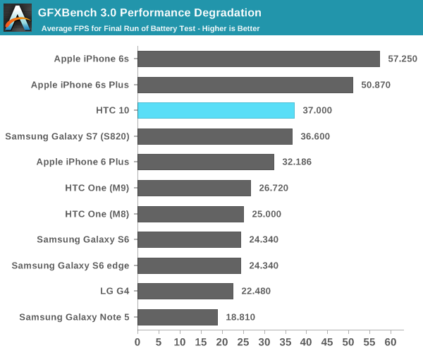
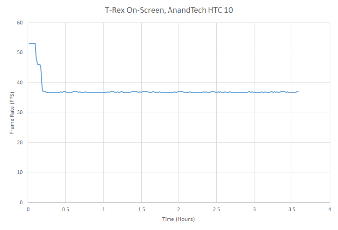

In GFXBench again we can see a similar sort of pattern in which the HTC 10 lasts about as long as the Galaxy S7, but in general it tends to throttle faster. However, it’s possible to see how the Galaxy S7’s throttling is best described as oddly configured as Samsung seems to prefer some oscillating behavior which negatively affects power efficiency before settling into steady state in the long run. It’s probably not a surprise that both have the same steady state as the back cover of the HTC 10 distributes heat quite evenly and both are roughly the same size. At any rate, the HTC 10 ends up being quite similar if you’re only comparing runtime and steady state frame rate, although the Galaxy S7 does manage to sustain more time before throttling down.
Whatever the case, overall battery life between the Galaxy S7 and HTC 10 are going to be similar, although how similar is going to be workload dependent and the bin of the SoC you end up getting. If your workload is almost purely display-bound, the Galaxy S7 seems to come out on top. If your usage is more mixed and primarily stresses the CPU like our 2016 web browsing test, the HTC 10 will edge out the Galaxy S7 and iPhone 6s by a nose. If you intend on running power viruses on your phone, it's likely that the bin of your SoC will matter more than anything else but runtime on both devices will be similar. Of course, due to the aluminum unibody limiting maximum skin temperatures the HTC 10 will probably start to throttle sooner but steady state performance should be similar. If you want a clear upgrade in battery life, basically the only choice at this time seems to be to go to a larger device like the Galaxy S7 edge.
Outside of battery life, one inevitable question is whether the HTC 10's eMMC is a detriment to the device. While this is by no means an exhaustive examination of storage performance, we can look at AndroBench 4 to get a good idea for performance. Unfortunately with Android 6 AndroBench 3.6 has broken timers yet again leading to wildly inaccurate figures for performance, and AndroBench 4 varies significantly from run to run for random read and write so for now we really can only disclose sequential figures with any level of confidence that these are comparable to AndroBench 3.6 and StorageBench performance figures.
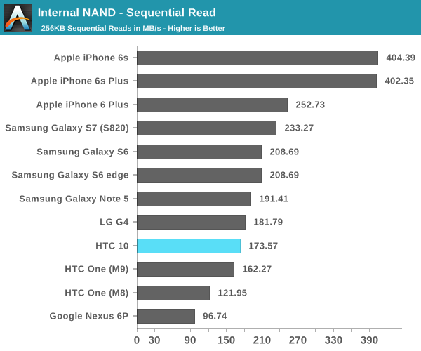
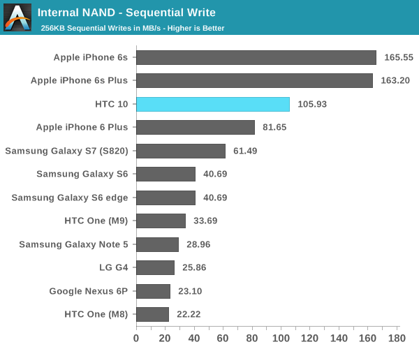
If you were fully expecting the HTC 10 to perform worse than the Samsung Galaxy S7 here like I was, you'll probably be surprised to learn that it doesn't actually do worse all the time. In this test at least, write performance of the HTC 10 is 75% greater than the Samsung MLC UFS solution in the Galaxy S7 due to the use of an SLC write cache. However, sequential reads on the Galaxy S7 are about 35% higher than what they are on the HTC 10. The same sort of pattern repeats itself in the random read and write tests for AndroBench 4, so at a high level it's pretty fair to say that things like burst camera photos, app updates, and similar write-intensive operations are going to be faster on the HTC 10, while read-intensive operations like loading apps may be slightly faster on the Galaxy S7 if storage reads are the critical path.
Overall, it's clear to me that the HTC 10 could be a contender for high end Android smartphones. If you were just to go down the spec sheet, it's probably fairly easy to conclude that HTC can't really go toe to toe with Samsung. However, with our tests so far there is a surprising amount of nuance to all of these comparisons that has to be considered. Battery life seems to be worse than the Galaxy S7 if you just consider display or SoC efficiency, but in a mixed use scenario HTC manages to close the gap. NAND performance seems to inevitably trail the Galaxy S7, but with the right eMMC selection HTC has a significant lead in write performance in all scenarios. In my experience, this seems to be the overall story of the HTC 10 thus far, although there are cases where one device is clearly superior to the other. Of course, this will have to wait for the full review, which should be in the near future.
Read More ...
Thunderbolt 3 in Action: Akitio Thunder3 Duo Pro DAS Review
A lot of attention has been paid to high-speed I/O interfaces for computing systems over the last five years. Flash-based storage media capable of multi-Gbps throughput have become very affordable. Display resolutions have also seen a rapid rate of increase. The necessity to support multiple such devices in both consumer and professional computing solutions have exposed the limitations of the traditional external I/O interfaces. Intel has been attempting to solve this problem with Thunderbolt Technology since 2011. Unfortunately, the uptake outside the Apple ecosystem for the first two versions has been minimal at best. The introduction of Thunderbolt 3, however, has been a game-changer. Systems and motherboards with Thunderbolt 3 support started coming to the market in late 2015. The first Thunderbolt 3 peripheral to appear in the market was the Akitio Thunder3 Duo Pro, a hardware RAID solution with two drive slots. Why do we think that Thunderbolt 3 is a game changer? How does the Akitio Thunder3 Duo Pro perform? What advantages does it deliver over other standard 2-bay hardware RAID solutions? Read on for our detailed analysis and review.
Read More ...
USB-C Authentication Tech to Restrict Usage of Uncertified USB-C Accessories and Cables
USB interconnections are expected to get more popular than ever thanks to convenience of reversible USB Type-C, its ability to deliver up to 100W of power and support for custom features. However, expanded functionality requires more sophisticated cables with multiple wires and special ID chips, which are more expensive to make than traditional USB cables. As it turned out in the recent months, many cheap cables are not compliant with USB-IF’s requirements; they either do not support high data-rates, cannot charge USB-C devices, or may even damage products they are connected to. The USB authentication promises to end frustrations and make future USB-C devices a little more secure, as an added bonus.
Devices compliant with the USB PD 3.0’s USB-C authentication tech will be able to verify capabilities of accessories compliant with the authentication technology and whether or not they have been certified by the USB-IF. The verification information will be exchanged right after devices are connected, before any data or energy is transferred. The USB-IF will make it possible to set up policies that will restrict usage of incompatible or uncertified accessories with particular host devices.
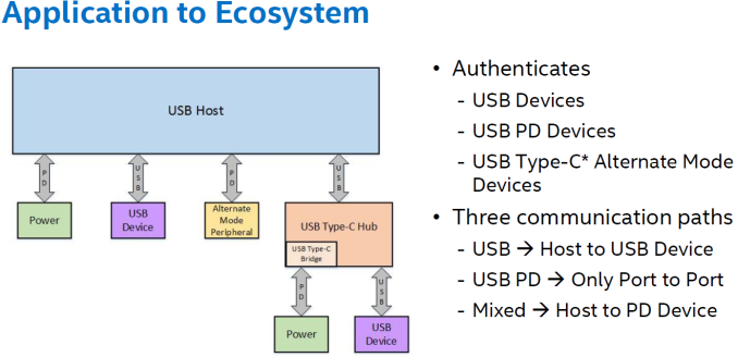
The USB-C authentication will divide accessories into three types: USB devices, USB power delivery devices (e.g., chargers) and USB Type-C alternate mode devices (e.g., displays). The authentication data messages will be transmitted using different communication paths (USB bus, USB PD or mixed) and will be encrypted using 128-bit methods.
| USB Type-C Authentication Cryptographic Methods | |
| Method | Use |
| Framework (ITU X.509) OID (ITU-T X.402) DER-encoding (ITU-T X.690) |
Certificate format |
| ECDSA (ANSI X9.62) using NIST P-256 curve (NIST-FIPS-186-4) | Digital signing of certificates and authenticationmessages |
| SHA256 (NIST-FIPS-180-4) | Hash algorithm |
| NIST-compliant PRNG source (SP800-90A) seeded with a 256-bit fullentropy value (SP800-90B) | Random numbers |
Based on what is known about the USB authentication, the technology can restrict usage of uncertified cables only in cases their usage is prohibited by manufacturers or end-users users themselves. Moreover, it will only be completely supported by fully-featured cables compatible with the USB Power Delivery 3.0 specifications, which will contain a chip with ID as well as optional vendor defined messages.
According to the USB-IF, it is possible to add the USB-C authentication protocol to host devices by updating their software and firmware, but that will depend on device manufacturers. Since it is not feasible to update things like chargers or cables, they will need to be replaced, or, their usage should be permitted by software-defined security policies. Owners of PCs, tablets and smartphones will be able to authorize only certain accessories to work with their devices, making it impossible to plug a USB flash drive to a host containing confidential data. Nonetheless, once an accessory is authorized, it will be able to work with hosts, harm them or even infect them with viruses. Therefore, the new USB technology is not a replacement for antiviruses.
It remains to be seen how different manufacturers take advantage of the new technology. If implemented too strictly, some hosts may get incompatible with the majority of cheap USB-C products on the market.
At present we do not know when the USB-IF plans to start certification of devices with the USB authentication technology and how the organization plans to certify thousands of cables and chargers. Perhaps, Intel, the company that developed the USB PD 3.0, will reveal more information at its IDF trade-show in the coming days, so, stay tuned.


Read More ...
The MSI Z170A SLI PLUS Review: Redefining the Base Line at $130
MSI’s motherboard range seems to expand every generation. Alongside the channel range, there’s the MSI Gaming, micro-ATX gaming, OC Certified, Krait, ECO, SLI PLUS, PC Mate and some I probably can’t think of. Each set can have a chipset mix, depending on their target market. The SLI PLUS line is relatively new, with the Z170A SLI PLUS in this review being the latest model. The goal of the SLI PLUS is form, function and application at a low price, with a few future-proof features and enough hardware for most PC enthusiasts systems. They seem to sell well, so we got a sample in to see the fuss. Two-word verdict: pleasantly surprised. Read on to see why.
Read More ...
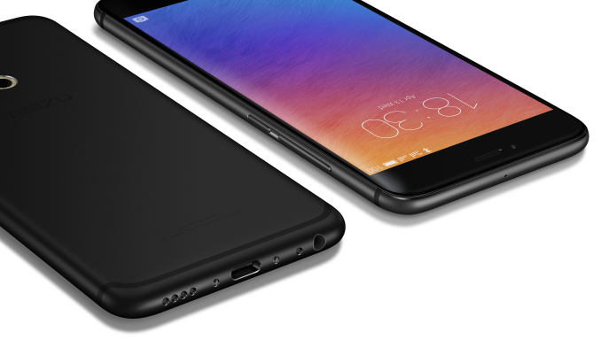
Meizu Announces New PRO 6
| Meizu PRO Series Specifications | ||
| Meizu PRO 6 | Meizu PRO 5 | |
| SoC | MediaTek Helio X25 2x A72 @ 2.5GHz 4x A53 @ 2.0GHz 4x A53 @ 1.4GHz Mali T880MP4 @ 850MHz |
Samsung Exynos 7420 4x A57 @ 2.1GHz 4x A53 @ 1.5GHz Mali T760MP8 @ 770MHz |
| RAM | 4GB LPDDR3-1866 | 3 / 4GB LPDDR4-3200 |
| NAND | 32 / 64GB eMMC 5.1 NAND | 32 / 64GB UFS 2.0 + microSD |
| Display | 5.2” 1080p AMOLED | 5.7” 1080p AMOLED |
| Modem | 2G/3G/4G LTE Cat 6 (Integrated MediaTek SoC Modem) |
2G/3G/4G LTE Cat 6 |
| Dimensions | 147.7 (h) x 70.8 (w) x 7.25 (d) mm 160g |
156.7 (h) x 78 (w) x 7.5 (d) mm 168g |
| Camera | Rear Camera 21.16MP ( 5444 x 4016 ) Sony IMX230 1/2.4" 1.12µm pixels F/2.2 aperture w/ Laser & Phase Detection focus |
Rear Camera 21.16MP ( 5444 x 4016 ) Sony IMX230 1/2.4" 1.12µm pixels F/2.0 aperture w/ Laser & Phase Detection focus w/ Dedicated Samsung ISP |
| Front Facing Camera 5MP 1.4µm pixels F/2.0 aperture |
Front Facing Camera 5MP 1.4µm pixels F/2.0 aperture |
|
| Battery | 2560mAh (~9.85 Whr) | 3050mAh (~11.74 Whr) |
| Launch OS | Android 6.0 with FlyMe 5.6 | Android 5.1 with FlyMe 5.0 |
| Connectivity | 802.11a/b/g/n 2.4 & 5GHz BT 4.1, GPS/GNSS USB-C 3.1 |
802.11 b/g/n/ac 2.4 & 5GHz BT 4.1 + BLE, GPS/GNSS USB-C |
| SIM Size | NanoSIM + NanoSIM | NanoSIM |
| Launch MSRP | 32GB RMB ¥2499 (USD~386, ~340€, ~271£) |
3GB/32GB RMB ¥2799 (USD~438, ~393€) |
| 64GB RMB ¥2799 (USD~432, ~381€, ~304£) |
4GB/64GB RMB ¥3099 (USD~485, ~435€) |
|
The PRO 6 is quite a strange successor as at first glance the upgrades aren't quite evident. The PRO 6 replaces the traditional Samsung LSI Exynos SoCs with MediaTek's Helio X25. The X25 is exclusive to the PRO 6 and essentially is an X20 with the dual-core A72 cluster clocked in at 2.5GHz instead of 2.3GHz. The three-cluster design also features a quad-core A53 at 2.0GHz as well as a low-power A53 quad-core at 1.4GHz. On the GPU side we see a Mali T880MP4 at 850MHz. Main memory is 4GB of LPDDR3 running at 933MHz.
The SoC choice puts the PRO 6 in a weird position when compared to the PRO 5 as except for single-thread performance the X25 should theoretically represent a downgrade compared to the Exynos 7420 in last year's model. It's especially in terms of power efficiency where this raises question as we move from a 14nm FinFET design back to a 20nm planar manufacturing process, so I hope that Meizu's SoC choice doesn't negatively impact power efficiency of the phone.
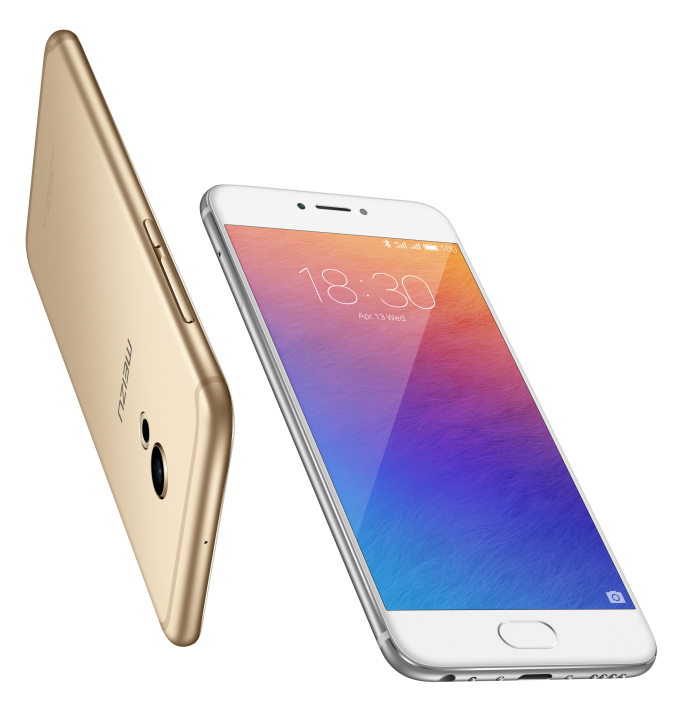
In terms of design the PRO 6 doesn't differ too much from the PRO 5, that is until one takes into account the form-factor of the new model. On the front we see very little distiguishable differences - except for the fact that Meizu downgraded the screen size from 5.7" down to 5.2" marking a departure from the larger "phablet" size. The display panel remains a 1080p AMOLED sourced by Samsung Display.
A first for Meizu is now the inclusion of a pressure sensitive touchscreen module which Meizu calls 3D Press. As we've seen in Apple's latest iPhones or even Huawei's implementation on the Mate S, this is a hardware feature that will undoubtedly depend on the software framework and applications to expose and take advantage of the new functionality. Meizu here might have some better lee-way in terms of Android customization when compared to other vendors who have to adhere to Google's CTS requirements, so it will be interesting to see what Meizu was able to come up with in the latest FlyMe 5.6 OS.
The reduction in size also has an impact on the integrated battery's capacity as we move from a 3050mAh cell down to a 2560mAh unit. Oddly enough, the device only loses 8g and remains relatively heavy for a 5.2" device, coming at 160g.
The main camera remains unchanged from the PRO 5, we find the same 21.16MP Sony IMX230 module featuring both PDAF as well as Laser auto-focus. We see a downgrade in the optics as the PRO 6 features an aperture of F/2.2 compared to the PRO 5's F/2.0 lens. The front-facing camera remains a 5MP unit with 1.4µm pixels.

The PRO 6 comes in 32GB or 64GB models RMB ¥2499 (USD~386, ~340€, ~271£) and RMB ¥2799
(USD~432, ~381€, ~304£) with pre-orders starting now.
Read More ...
Micron Presents New SSDs and Strategy: From Components to Whole Solutions, 3D NAND Shipping Imminent
The reference architectures are branded as Micron Accelerated Solutions, the first of which is a hardware platform by Supermicro bundled with VMWare Virtual SAN and using Micron M510DC SSDs. A similar solution has been developed with the Ceph object storage system and work is underway with Nexenta on an integrated system that will be available in the second half of the year.
In addition to the whole-system products, Micron shared information about several new and upcoming SSDs. The 9100 and 7100 series PCIe SSDs were launched and covered in a separate post. The 9100 was featured in a demo of the software defined storage system under development by SymbolicIO. The 7100 series is the second product line resulting from Micron's collaboration with Seagate, which previously resulted in a family of SAS SSDs.
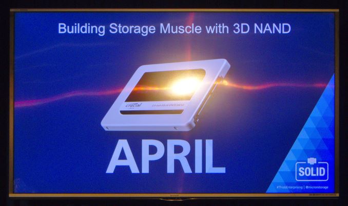
Micron announced the schedule for their first 3D NAND SSDs. The Crucial MX300 will launch later this month using Micron's 3D TLC NAND. Specifics aren't available yet, but given the 384Gbit (48GB) capacity per die of the 3D TLC, the MX300 will either feature oddball capacities, significantly more overprovisioning than its MLC-based predecessors, or an uneven distribution of NAND dies across the controller's channels.
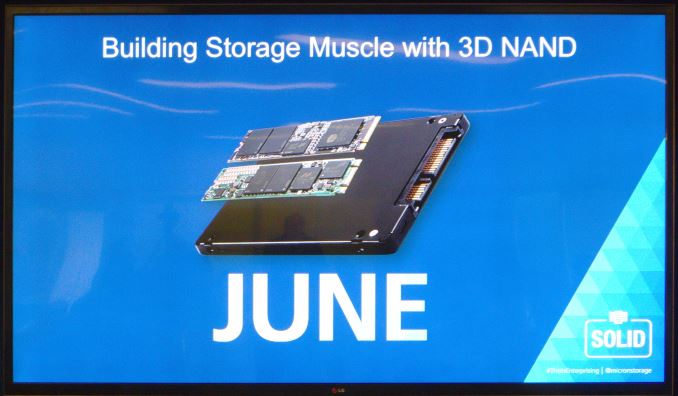
In June Micron will launch a pair of OEM client SSDs, the 1100 series and the 2100 series. Specifications for those drives were also not announced, but the photographs reveal some details: an M.2 SATA drive using a Marvell controller (probably 88SS1074, and thus probably also using TLC), and an M.2 PCIe drive with a Silicon Motion controller, presumably the SM2260.
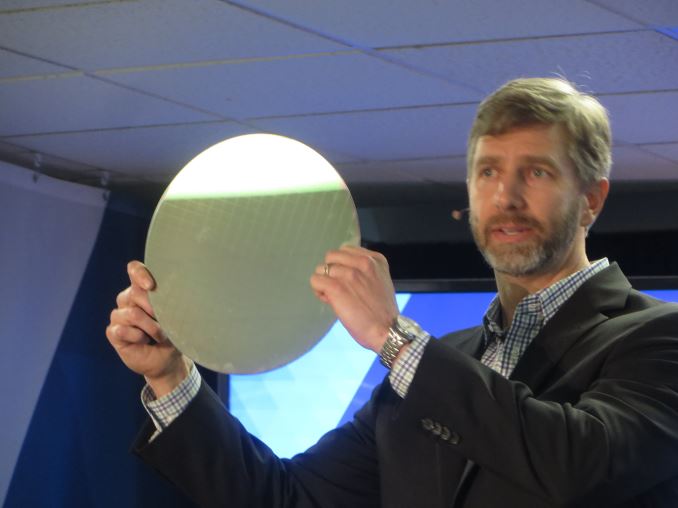
Micron says there will be 3D NAND for the datacenter in the second half of the year, but they have not yet identified any of the drives that will be using it. A 3D XPoint wafer was waved around onstage but Micron made no substantial announcements today about the technology. They did promise that we'll be hearing more about the products and their branding later this year, and confirmed that they've been focusing on using 3D XPoint in NVMe products (whereas Intel is also developing NVDIMMs).


Read More ...
Several CAPI-Enabled Accelerators for OpenPOWER Servers Revealed
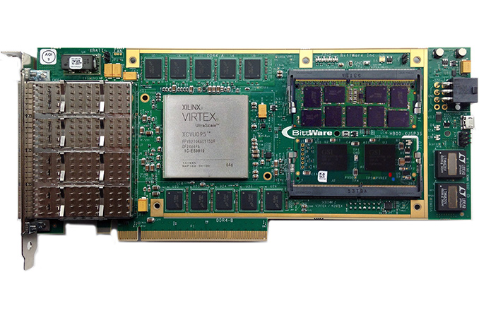
IBM’s CAPI port is a PCIe 3.0-based interconnection specifically designed for programmable processors (e.g., ASICs, GPUs, FPGAs, etc.) that enables them to address the same memory address space as the CPU. CAPI requires custom hardware incorporated into IBM’s POWER8 processors, which is called the coherent accelerator processor proxy (CAPP), as well as a POWER service layer (PSL) integrated into CAPI-supporting processors. CAPP maintains a directory of cache lines held by the accelerator and snoops the processor bus for the accelerator. The PSL performs address translations and holds the coherent data for quick access by the accelerating hardware. To work, CAPI has to be supported by the hardware, the operating system and the application in use. At present, IBM’s POWER8 CPUs, a number of accelerators, RedHat Enterprise Linux 7.2 LE (and higher), and Ubuntu LE, as well as select programs, support CAPI.
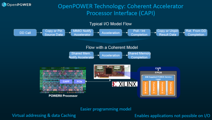
IBM and the OpenPOWER Foundation need CAPI in order to enable a relatively simple and inexpensive way to build special-purpose accelerators for various workloads. The aim is to make POWER8-based machines viable for a variety of market segments as well as to create platforms that can process modern workloads faster.
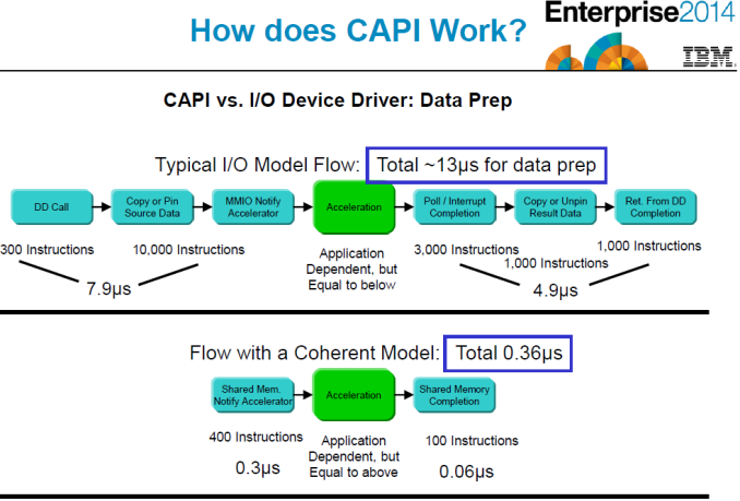
While it is possible to enable unified memory for CPUs and co-processors using custom hardware and multiple tweaks in device drivers, this requires huge investments in silicon development, complex drivers and a number of other things. By contrast, programming an FPGA (field-programmable gate array) is considerably cheaper, and the CAPI technology brings them key heterogeneous processing capabilities. While this does not necessarily enable higher bandwidth between the CPU and the accelerator (after all, CAPI is layered on top of PCI Express 3.0 and a specified peak bandwidth), according to IBM they remove overheads, improve performance and can potentially simplify the workflow for programmers. In short, CAPI is an important part of IBM’s POWER strategy in general as well as OpenPOWER initiative.
At this year’s OpenPOWER Summit, IBM and its partners revealed over a dozen of special-purpose CAPI-enabled FPGA-based accelerators. This shows that the OpenPOWER platform is gaining interest and investment from different sources. The list of developers includes such companies as BittWare, DRC, IBM, Mellanox, Xilinx and others, but some decided not to publish details about their accelerators, as it seems from OpenPOWER’s press release. The accelerators revealed at the conference are either available or are set to become available in the coming quarters. The devices come in the form of PCIe 3.0 x8 or x16 cards and are compatible with IBM POWER8-based servers. Some are also compatible with machines running other processors (and in this case, CAPI is not supported).
| IBM CAPI-Compatible Accelerators | |||||
| Developer | Model | Hardware and Application | |||
| Alpha Data | ADM-PCIE-8K5 | Xilinx UltraSCALE KU115-2 FPGA 2×8 GB of DDR4-2400 with ECC (32 GB version can be built) Dual Firefly connectors for up to 4×16Gbps per connector Reconfigurable accelerator for custom video processing, machine learning, HPC and network acceleration applications. Available as add-in PCIe 3.0 x8 cards. |
|||
| BittWare | XUSP3S | Xilinx Virtex UltraScale 80/95/125/160/190 or Kintex UltraScale 115 2×16 GB DDR4 ECC (64 GB version can be built), QDR memory Four QSFP28 cages for 1×400GbE, 4×100GbE, 4×40GbE, 16×25GbE, or 16×10GbE Massive data flow and packet processing. Available as add-in PCIe 3.0 x16 cards. |
|||
| DRC | GraphFind | Xilinx Kintex UltraScale KU115 FPGA Can rapidly discover relationships between people, places, events, and objects. Simultaneously identifying focal points with weighted strengths of connections. Available as a PCIe card, or as a pre-configured appliance consisting of multiple cards. |
|||
| DRC | Novara | Xilinx FPGA A search engine and an accelerator, which identifies key imprecise phrases and Bit patterns using a fuzzy logic analyzer that can instantly analyze millions of messages and data streams without the need to index first. Can process up to 2.5 GB of data per second. Available as 1U server, which contains up to four Novara cards. Servers can be clustered. |
|||
| DRC | Ferrara2 | Xilinx FPGA, four QSFP28 cages. Encrypts and/or authenticates data using AES-256 algorithm with bit-splitting capability from Security First Corporation (SFC) at line rates up to 40 Gb/s. Available as PCIe 3.0 x16 add-in boards for servers, communication or storage systems. Multiple Ferrara2 boards can be placed in one system. |
|||
| Edico Genome | DRAGEN Genomics Platform | Xilinx Virtex-7 980T FPGA 4×4 GB DDR3L-1866 memory. Analyzes an entire human genome in 26 minutes (vs. 30 hours on general-purpose hardware). Enables healthcare providers to identify patients at higher risk for cancer before the conditions worsen. Compatible with the IBM S822LC server. Available in a pre-configured Power8 server. |
|||
| IBM | Prototype | Xilinx Virtex UltraScale 190 16 GB of Micron HMC memory. Acceleration of in-memory computing applications. Available as add-in PCIe 3.0 x16 cards. |
|||
| IBM, Nallatech, RedisLabs Altera |
IBM Data Engine for NoSQL | IBM Power S822L server(s) IBM FlashSystem 840 or 900 all-Flash storage system(s) Altera Stratix V FPGA-based interconnection card with 10 GbE SFP+ ports by Nallatech IBM FlashSystems are attached to the POWER8 processor through the CAPI coherent attach card. Thanks to the new interconnection method, the Redis Enterprise Cluster application can issue read/write commands that eliminate 97% of the code path length. According to IBM, this enables IBM Data Engine for NoSQL to access Flash within latency levels comparable to traditional RAM-based x86 implementations. Various configurations available. |
|||
| IBM, Nallatech, Samsung, Xilinx | Prototype | Xilinx FPGA 2×1 TB Samsung M.2 NVMe SSDs. IBM Data Engine for NoSQL, which allows fast application exploitation in a smaller, in-server form-factor. Available as add-in PCIe 3.0 x8 cards. |
|||
| Mellanox | ConnectX-4 VPI | ConnectX-4 VPI ConnectX-4 adapter cards with virtual protocol interconnect (VPI) support EDR 100 Gb/s InfiniBand and 100 Gb/s Ethernet connectivity. Available as add-in PCIe 3.0 x16 cards. |
|||
| Semptian | NSA-120 NSA-120B |
Xilinx Kintex UltraScale XCKU060/XVKU115 2×4 GB or 2×8 GB DDR3-1600 memory with ECC Two SATA interfaces Network and service accelerator. Can be used in big data analysis, image recognition/processing, video encoding/decoding, data compression/decompression, data encryption/decryption, voice recognition, neural network, machine learning, network security, etc. Available as add-in PCIe 3.0 x8 cards. |
|||
One of the important announcements at the summit was Edico Genome’s DRAGEN genomics platform, which uses an accelerator powered by the Xilinx Virtex-7 980T FPGA and is equipped with 16 GB of quad-channel DDR3L-1866 memory. The platform, which is based on a 2-way IBM S822LC server, can analyze an entire genome in 26 minutes, down from approximately 30 hours on general-purpose processors. An earlier prototype was shown at SuperComputing 2015, however this seems to be the announcement of the full product.
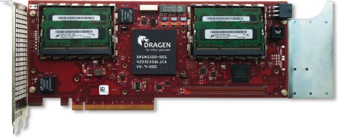
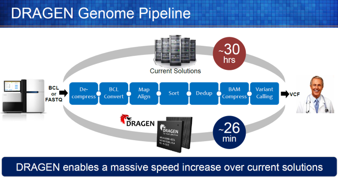
Other interesting solutions discussed at the summit include an FPGA-based accelerator for discovering relationships hidden in big data; an FPGA-powered fuzzy search engine for imprecise string searching and matching, which can analyze millions of messages and data streams without indexing; as well as various reconfigurable accelerators for HPC, Big Data, and so on. IBM also mentions that there are companies offering CAPI-enabled building blocks for FPGAs for computer vision, machine learning, and other applications. Some of those companies are startups or working in stealth mode (we do not know whether they developed their building blocks thanks to the SuperVessel program, though this is a possibility), and they may announce their products over time.
While the number of CAPI-enabled accelerators available today is not high, it is growing, which is a good news for the OpenPOWER ecosystem. Positive news (from IBM) is the number of China-based companies developing accelerators featuring CAPI, which shows that local companies in growing markets for servers are expressing interest in such solutions.
Read More ...
Micron Announces 9100 & 7100 Series PCIe Enterprise SSDs
The new Micron 9100 NVMe PCIe SSD series is the high-performance and high-capacity product. Capacity ranges from 800GB to 3.2TB in either half-height half-length add-in card form factor or as a 15mm thick 2.5" U.2 drive. With a TDP of up to 27W, the Micron 9100 SSD is the more direct successor to the P420m and is using a PMC-Sierra controller that is descended from the controller used in Micron's previous PCIe SSDs.
| Micron 9100 PCIe SSD Specifications | |||||
| Capacity | 800GB | 1.2TB | 1.6TB | 2.4TB | 3.2TB |
| Interface | PCIe 3.0 x4 HHHL or U.2 | ||||
| Sequential Read | 2.1 GB/s | 2.8 GB/s | 2.8 GB/s | 3.0 GB/s | 3.0 GB/s |
| Sequential Write | 650 MB/s | 1.3 GB/s | 1.3 GB/s | 2.0 GB/s | 2.0 GB/s |
| Random Read IOPS | 540k | 700k | 700k | 750k | 750k |
| Random Write IOPS | 55k | 180k | 100k | 300k | 160k |
| Idle Power Consumption | 7W | ||||
| Active Power Consumption | 16W | 21W | 21W | 27W | 27W |
The Micron 7100 NVMe PCIe SSD expands Micron's offerings into a more mainstream segment of the market by adopting Marvell's 88SS1093 controller that is designed for client and smaller enterprise drives. Capacities for the 7100 range from 400GB to 960GB for the M.2 version and from 400GB to 1.9TB as a 7.5mm thick 2.5" U.2 drive. The smaller Marvell controller will keep power consumption below 12.5W and the M.2 version further throttles to a limit of 8.25W.
| Micron 7100 PCIe SSD Specifications | ||||||
| Capacity | 400GB | 480GB | 800GB | 960GB | 1.6TB | 1.92TB |
| Interface | M.2 22110 or 2.5" U.2 | 2.5" U.2 | ||||
| Sequential Read | 2.4 GB/s | 2.5 GB/s | 2.5 GB/s | |||
| Sequential Write | 475 MB/s (M.2) 500 MB/s (U.2) |
600 MB/s (M.2) 900 MB/s (U.2) |
900 MB/s | |||
| Random Read IOPS | 180k | 220k | 235k | |||
| Random Write IOPS | 25k | 10k | 33k | 12k | 40k | 15k |
| Idle Power Consumption | 3.7W | |||||
| Maximum Power Consumption | 8.25W (M.2) 12.5W (U.2) |
12.5W | ||||
Both the 9100 and 7100 series include models in two tiers of overprovisioning: for read-heavy or mixed workloads. The drives with greater overprivisioning sacrifice some capacity for greatly increased random write speeds and improved write endurance, though specifications for the latter have not yet been released.
Read More ...
Plextor Embraces TLC NAND: Introduces M7V SSD
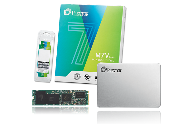
Plextor demonstrated its first TLC-powered drive back at CES 2015. At the time, the SSD was based on the Marvell 88SS1074 controller with LDPC (low-density parity check) error correction for increased endurance as well as Toshiba’s TLC NAND made using its second-generation 19 nm process technology (A19 nm). As it appears, that drive was not the only low-cost option considered by Plextor. By the time company needed to ramp up production of its affordable SSD in mid-2015, it decided to postpone the release of its TLC-powered drive. Instead, the company introduced the M6V, which features Toshiba’s 15 nm MLC NAND, but is powered by a low-cost quad-channel Silicon Motion's SM2246EN controller. As a result, Plextor managed to release a value SSD, but kept using familiar MLC memory (albeit, with a new controller).
Nonetheless, Plextor knew it could not to skip planar TLC NAND (and use 3D NAND once it becomes available instead), which is why it continued to work on its TLC drives. This month, the company finally revealed its first TLC-based product — the M7V.
Marvell’s 88SS1074 Gets a New Version
The Plextor M7V SSDs are based on the Marvell 88SS1074B1 controller as well as Toshiba’s TLC flash memory made using its 15 nm process technology. When Marvell originally introduced its 88SS1074 controller in May, 2014, it emphasized that the chip was specifically designed to enable SSD makers to use TLC NAND, which is why it features its own NANDEdge error correction technology based on LDPC algorithms. Plextor has been working on products featuring this controller for a long time and the M7V is the fruit of this work.
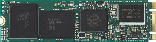
For some reason, Plextor calls the 88SS1074B1 “the next-generation controller”, even though it looks like a new version of the chip introduced two years ago. This is not a bad thing in general because the 88SS1074 is a fine 8-channel NAND controller and Plextor’s engineers should be familiar with it (after a couple of years of playing with it). If the B1 version has higher clock-rates and/or more processing cores, it can perform more error correction and other operations, which potentially can improve endurance, reliability and/or performance of SSDs. In fact, the new revision of the chip could be the key to many technologies Plextor incorporated into the M7V.
By The Numbers
Plextor will offer its M7V family of SSDs in 2.5”/7mm (PX-M7VC) and M.2 2280 (PX-M7VG) form-factors. In the case of the latter, this is a SATA M.2 drive, as the Marvell 88SS1074B1 controller only supports SATA.
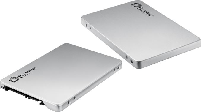
Plextor will offer M7V in 128 GB, 256 GB and 512 GB configurations. The drives also come with enlarged DRAM buffers, which are important for performance and, possibly, for Plextor’s way of handling TLC memory.
Plextor claims that maximum sequential read speed of an M7V SSD is 560 MB/s, whereas its maximum sequential read speed is 530 MB/s. Maximum random 4K read/write speed declared by the manufacturer is 98000/84000 IOPS.
| Plextor M7V and M6V SSD Specifications | ||||||
| Size | 128 GB | 256 GB | 512 GB | 128 GB | 256 GB | 512 GB |
| Controller | Marvell 88SS1074B1 | Silicon Motion SM2246EN | ||||
| NAND | Toshiba 15 nm Toggle TLC | Toshiba 15nm Toggle MLC | ||||
| DRAM Cache | 256 MB | 512 MB | 1GB | 128 MB | 256 MB | 512 MB |
| Sequential Read | 560 MB/s | 535 MB/s | ||||
| Sequential Write | 500 MB/s | 530 MB/s | 170 MB/s | 335 MB/s | 455 MB/s | |
| 4kB Random Read | 97K IOPS | 98K IOPS | 81K IOPS | 83K IOPS | 83K IOPS | |
| 4kB Random Write | 51K IOPS | 84K IOPS | 42K IOPS | 80K IOPS | 80K IOPS | |
| Warranty | 3 years | |||||
It is interesting to note that Plextor’s M7V SSDs are rated faster than the company’s M6V drives both in terms of sequential read/write operations (keep in mind that we are dealing with TLC-based storage devices, hence, we’ll talk about their writing performance below) as well as random read/write operations. Therefore, despite of getting a drive with cheaper memory, owners of the M7V may get higher performance if Plextor's performance numbers prove true.


Enhanced Endurance & PlexNitro
Plextor claims that it uses TLC NAND memory from Toshiba with increased endurance (which it calls “top-class components”). It also says that its exclusive firmware along with flash components help to increase maximum amount of memory’s P/E cycles to 2000, which is higher compared to that of typical TLC NAND. In fact, durability is what Plextor sees as the main selling point of the M7V.
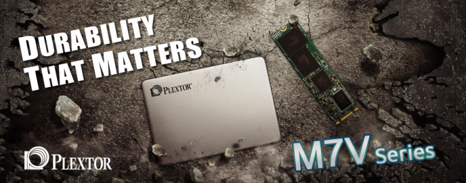
The company does not specify whether it uses Toshiba’s new TLC NAND devices that architecturally have higher endurance (an unlikely scenario), or Marvell’s 88SS1074B1 controller with LDPC-based error correction technology. Similarly, they aren't saying much about their own firmware, with its own set of tricks. For competitive reasons, Plextor does not specify the amount of NAND used for over-provisioning to increase endurance of its drives (but not components themselves), but extra NAND helps to increase durability of SSDs.
To speed up writing performance of TLC NAND-based SSDs, like most other TLC drive vendors Plextor is employing a write acceleration technology of some kind to speed up write operations, which it calls PlexNitro. The standard here for TLC drives is to implement a pseudo-SLC mode write cache, however it's not clear if this is what Plextor is doing. The uncertainty comes from the fact that Plextor isn't setting aside space for the pSLC cache like other TLC drives have, and is why the M7V ships at 128/256/512GB rather than 120/240/480GB. Whether this means that they're instead dipping into the traditional and innate ~7% spare area pool or something else entirely remains to be seen.
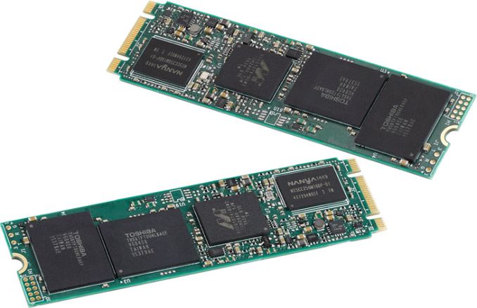
The actual peculiarities of PlexNitro are yet to be discovered, but what Plextor promises - consistently high performance, increased capacities and high endurance - sounds impressive. Still, it's something we'll have to validate once we're able to benchmark the drive and dive deeper into the workings of PlexNitro.
Finally, the new Plextor M7V solid-state storage devices should hit the market later this month. Plextor did not specify recommended prices of its M7V SSDs, but it is logical to expect them to cost less than the company’s MLC-based M6S Plus drives introduced several weeks ago. The Plextor M7V SSDs offer MTBF of up to 1.5 million hours and are covered with a limited three-year warranty.
Read More ...
Hands On With The HTC 10: A Fresh Start
At this point it’s probably not a secret that HTC has been struggling for the past few years. While the One M8 was a solid upgrade to the One M7, it was unfortunate in the sense that it did not resolve the problems that the M7 had. HTC made a leap in extending the One's core strengths of an aluminum unibody design, dual front-facing speakers, and generally polished user experience, but they left other matters unresolved. More frustratingly, with the One M9 it seemed that HTC had taken a step back as there was very little that had meaningfully changed, and it wasn’t entirely unusual to see changes that were a regression relative to the One M8. To be honest, I was ready to write off HTC entirely from the market as the One M9+ felt like it was just more of the same mistakes from HTC.
To see if the HTC 10 is more of the same, read on for the full article.
Read More ...
Available Tags:Intel , Apple , MacBook , Western Digital , AMD , ASUS , SSD , FirePro , GIGABYTE , GeForce , GTX , HTC , Thunderbolt , MSI , 3D ,
No comments:
Post a Comment