
AMD Releasing New Crimson Drivers for GPU Fan Issue (Update: Released)
Original: Last week we covered the launch of AMD’s new Radeon software known as Crimson. Crimson is a departure from the Catalyst name, offering an updated interface and promising a larger range of quality assurance testing moving into the new DX12 era. Part of this includes several new features, and it’s worth reading into Ryan and Daniel’s piece on the new software. Despite the best intentions, it happens that this new driver also comes with a few issues that are leaving some users concerned.
As reported in this Reddit thread over at /r/pcmasterrace, the new drivers are causing some graphics cards to adopt an abnormal fan profile, limiting the fan speed to a maximum of 20% by default. As a result, during workloads that require the graphics card, the components on the card are heating up faster than intended. It should be noted that the extent of this issue is hard to determine at this point, as a random spread of users seem to be affected right now.
Technically this should result in the GPU hitting thermal limits and causing the chip to reduce the voltage and frequency, though according to these reports it seems that some of the affected cards are failing, either as a result of VRM overheating or other board design issues relating to high temperatures, even if the GPU throttles down, because of the low fan speed. So despite the GPU throttling, the sustained power draw combined with the low fan speed still increases the temperature, and rather than trip some sort of fail-over giving a BSOD, some GPUs seem to have components that are susceptible to the temperature before a fail-over kicks in.
Some users are reporting that this is a global overdrive setting fixed in the software, which can be re-enabled by following these instructions to remove the 20% fan speed limit. However this hotfix requires re-enabling every time the system is restarted. The fan speed should also be able to be changed using third party software (MSI Afterburner, EVGA PrecisionX).
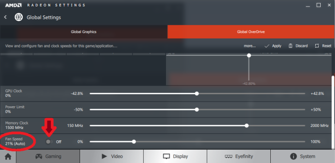
Instructions from /u/Mufinz1337: 'Make sure it states OFF if you want your fan speeds to be automatic'
We received an email late last night from AMD stating that the problem has been identified and an update to the drivers will be available at some point today, Monday 30th November.
The problem seems to revolve around system configurations that seem confusing to the initial release of the Crimson software, resulting in an odd initial fan setting that is fixed when the software initialises (although it seems to be a random assortment of GPUs affected, even for those with seemingly straightforward systems). Some users have reported their cards have permanently failed, although the exact causes as to why are unknown at this point. We have seen reports pointing to VRM quality of cheaper cards being poor outside the specified temperature window, though at this point we have not heard of any OEM releasing a statement regarding replacement – users with cards in warranty should under normal circumstances be able to get their cards replaced with their retailer, and it will be up to the retailer/OEM to manage the issue further up the chain with distribution.
For users affected, they can either do the manual fan adjustment each time they boot their system, roll back drivers via DDU, or wait for the driver update later today. We will post links here when we get them.
We
are aware of low fan speed reports on select GPUs with Radeon Software
Crimson Edition. We intend to publish a hotfix on Monday.
— AMD Radeon Graphics (@AMDRadeon) November 29, 2015
Read More ...
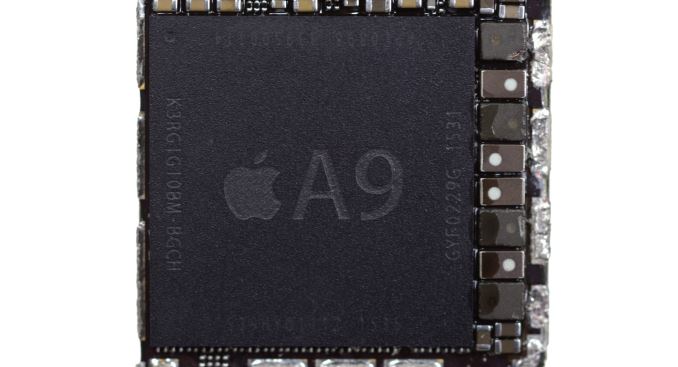
Correcting Apple's A9 SoC L3 Cache Size: A 4MB Victim Cache
In our original analysis of the A9, I wrote that the L3 cache was 8MB. This was based upon our initial tests along with Chipworks’ own analysis of the physical layout of the A9, which pointed to an 8MB L3 cache. Specifically, at the time I wrote:
However it’s also worth mentioning that as Apple is using an inclusive style cache here – where all cache data is replicated at the lower levels to allow for quick eviction at the upper levels – then Apple would have needed to increase the L3 cache size by 2MB in the first place just to offset the larger L2 cache. So the “effective” increase in the L3 cache size won’t be quite as great. Otherwise I’m a bit surprised that Apple has been able to pack in what amounts to 6MB more of SRAM on to A9 versus A8 despite the lack of a full manufacturing node’s increase in transistor density.
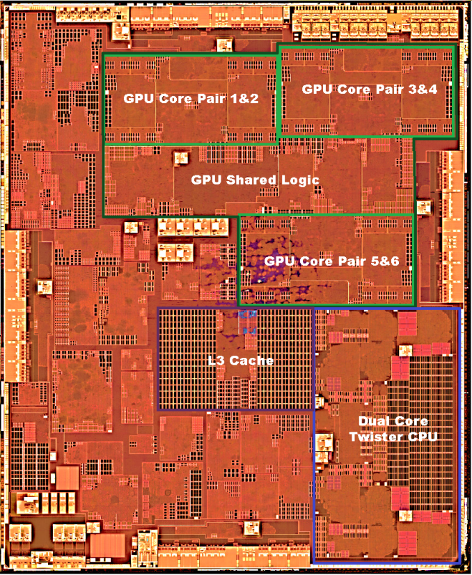
As it turns out, 8MB of cache was too good to be true. After a few enlightening discussions with some other individuals, some further testing, and further discussions with Chipworks, both our performance analysis and their die analysis far more strongly point to a 4MB cache. In particular, Chipworks puts the physical size of the TSMC A9 variant’s L3 cache at ~4.5mm2, versus ~4.9mm2 for A8’s L3 cache. Ultimately TSMC’s 16nm FinFET process is built on top of their 20nm process – the metal pitch size as used by Apple is the same with both processes – and this is the limiting factor for the L3 cache SRAM density.
| Apple SoC Comparison | ||||||
| A9X | A9 | A8 | A7 | |||
| CPU | 2x Twister | 2x Twister | 2x Typhoon | 2x Cyclone | ||
| CPU Clockspeed | 2.26GHz | 1.85GHz | 1.4GHz | 1.3GHz | ||
| GPU | PVR 12 Cluster Series7 | PVR GT7600 | PVR GX6450 | PVR G6430 | ||
| RAM | 4GB LPDDR4 | 2GB LPDDR4 | 1GB LPDDR3 | 1GB LPDDR3 | ||
| Memory Bus Width | 128-bit | 64-bit | 64-bit | 64-bit | ||
| Memory Bandwidth | 51.2GB/sec | 25.6GB/sec | 12.8GB/sec | 12.8GB/sec | ||
| L2 Cache | 3MB | 3MB | 1MB | 1MB | ||
| L3 Cache | None | 4MB (Victim) | 4MB (Inclusive) | 4MB (Inclusive) | ||
| Manufacturing Process | TSMC 16nm FinFET | TSMC 16nm & Samsung 14nm |
TSMC 20nm | Samsung 28nm | ||
But what is perhaps more interesting is what Apple is doing with their 4MB of L3 cache. An inclusive cache needs to be larger than the previous (inner) cache level, as it contains a copy of everything from the previous cache level. On A8 this was a 4:1 ratio, whereas with A9 this is a 4:3 ratio. One could technically still have an inclusive L3 cache with this setup, but the majority of its space would be occupied by the copy of the A9’s now 3MB L2 cache.
So what has Apple done instead? Inlight of Chipworks’ reassessment of the A9’s L3 cache size it’s clear that Apple has re-architected their L3 cache design instead.
What I believe we’re looking at here is that Apple has gone from an inclusive cache on A7 and A8 to a victim cache on A9. A victim cache, in a nutshell, is a type of exclusive catch that is filled (and only filled) by cache lines evicted from the previous cache level. In A9’s case, this means that items evicted from the L2 caches are sent to the L3. This keeps recently used data and instructions that don’t fit in the L2 cache still on-chip, improving performance and saving power versus having to go to main memory, as recently used data is still likely to be needed again.
The shift from an inclusive cache to a victim cache allows the 4MB cache on A9 to still be useful, despite the fact that it’s now only slightly larger than the CPU’s L2 cache. Of course there are tradeoffs here – if you actually need something in the L3, it’s more work to manage moving data between L2 and L3 – but at the same time this allows Apple to retain many of the benefits of a cache without dedicating more space to an overall larger L3 cache.
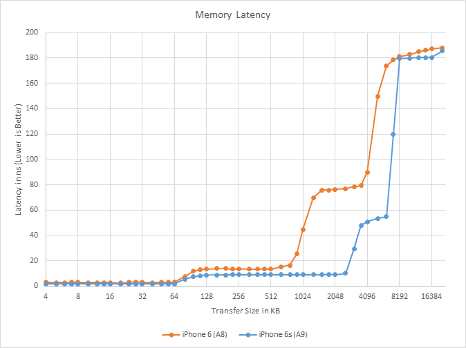
Meanwhile from the software side we can validate that it’s a victim cache by going back to our A9 latency graph. With the exclusive nature of the victim cache, the effective range of the L3 cache on A9 is the first 4MB after the end of the L2 cache; in other words, the L3 cache covers the 3MB to 7MB range in this test. Looking at our results, there’s a significant jump up in latency from 7MB to 8MB. Previously I had believed this to be due to the fact that our testing can’t control everything in the cache – the rest of the OS still needs to run – but in retrospect this fits the data much better, especially when coupled with Chipworks’ further analysis.
Ultimately the fact that Apple made such a significant cache change with A9 is more than I was expecting, but at the same time it’s worth keeping in mind that the L3 cache was only introduced back alongside Cyclone (A7) to begin with. So like several other aspects of Apple’s SoC design, A9 is very much an Intel-style “tock” on the microarchitecture side, with Apple having made significant changes to much more than just the CPU. Though coupled with what we now know about A9X, it does make me wonder whether Apple will keep around the L3 victim cache for A10 and beyond, or if it too will go the way of A9X’s L3 cache and be removed entirely in future generations.
Read More ...
More on Apple’s A9X SoC: 147mm2@TSMC, 12 GPU Cores, No L3 Cache
A9X is the first dedicated ARM tablet SoC to be released on a leading-edge FinFET process, and it’s being paired with Apple’s first large-format tablet, which in some ways changes the rules of the game. Apple has to contend with the realities of manufacturing a larger SoC on a leading-edge process, and on the other hand a larger tablet that’s approaching the size of an Ultrabook opens up new doors as far as space and thermals are concerned. As a result while we could make some initial educated guesses, we’ve known that there would be a curveball in A9X’s design, and that’s something we couldn’t confirm until the release of Chipworks’ die shot. So without further ado:
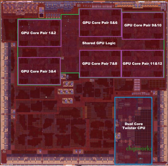
A9X Die Shot w/AT Annotations (Die Shot Courtesy Chipworks)
| Apple SoC Comparison | ||||||
| A9X | A9 | A8X | A6X | |||
| CPU | 2x Twister | 2x Twister | 3x Typhoon | 2x Swift | ||
| CPU Clockspeed | 2.26GHz | 1.85GHz | 1.5GHz | 1.3GHz | ||
| GPU | PVR 12 Cluster Series7 | PVR GT7600 | Apple/PVR GXA6850 | PVR SGX554 MP4 | ||
| RAM | 4GB LPDDR4 | 2GB LPDDR4 | 2GB LPDDR3 | 1GB LPDDR2 | ||
| Memory Bus Width | 128-bit | 64-bit | 128-bit | 128-bit | ||
| Memory Bandwidth | 51.2GB/sec | 25.6GB/sec | 25.6GB/sec | 17.1GB/sec | ||
| L2 Cache | 3MB | 3MB | 2MB | 1MB | ||
| L3 Cache | None | 4MB | 4MB | N/A | ||
| Manufacturing Process | TSMC 16nm FinFET | TSMC 16nm & Samsung 14nm |
TSMC 20nm | Samsung 32nm | ||
Die Size: 147mm2, Manufactured By TSMC
First off, Chipworks’ analysis shows that the A9X is roughly 147mm2 in die size, and that it’s manufactured by TSMC on their 16nm FinFET process. We should note that Chipworks has only looked at the one sample, but unlike the iPhone 6s there’s no reason to expect that Apple is dual-sourcing a much lower volume tablet SoC.
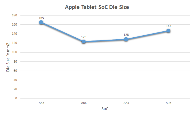
At 147mm2 the A9X is the second-largest of Apple’s X-series tablet SoCs. Only the A5X, the first such SoC, was larger. Fittingly, it was also built relative to Apple’s equally large A5 phone SoC. With only 3 previous tablet SoCs to use as a point of comparison I’m not sure there’s really a sweet spot we can say that Apple likes to stick to, but after two generations of SoCs in the 120mm2 to 130mm2 range, A9X is noticeably larger.
Some of that comes from the fact that A9 itself is a bit larger than normal – the TSMC version is 104.5mm2 – but Apple has also clearly added a fair bit to the SoC. The wildcard here is what yields look like for Apple, as that would tell us a lot about whether 147mm2 is simply a large part or if Apple has taken a greater amount of risk than usual here. As 16nm FinFET is TSMC’s first-generation FinFET process, and save possibly some FPGAs this is the largest 16nm chip we know to be in mass production there, it’s reasonable to assume that yields aren’t quite as good as with past Apple tablet SoCs. But whether they’re significantly worse – and if this had any impact on Apple’s decision to only ship A9X with the more expensive iPad Pro – is a matter that we’ll have to leave to speculation at this time.
Finally, it's also worth noting just how large A9X is compared to other high performance processors. Intel's latest-generation Skylake processors measure in at ~99mm2 for the 2 core GT2 configuration (Skylake-Y 2+2), and even the 4 core desktop GT2 configuration (Intel Skylake-K 4+2) is only 122mm2. So A9X is larger than either of these CPU cores, though admittedly as a whole SoC A9X contains a number of functional units either not present on Skylake or on Skylake's Platform Controller Hub (PCH). Still, this is the first time that we've seen an Apple launch a tablet SoC larger than an Intel 4 core desktop CPU.
GPU: PVR 12 cluster Series7
One thing we do know is that Apple has invested a lot of their die space into ramping up the graphics subsystem and the memory subsystem that feeds it. Based on our original benchmark results of the A9X and the premium on FinFET production at the moment, I expected that the curveball with A9X would be that Apple went with a more unusual 10 core PowerVR Series7 configuration, up from 6 cores in A9. Instead, based on Chipworks’ die shot, I have once again underestimated Apple’s willingness to quickly ramp up the number of GPU cores they use. Chipworks’ shot makes it clear that there are 12 GPU cores, twice the number found in the A9.
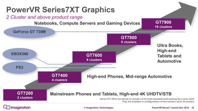
In Imagination’s PowerVR Series7 roadmap, the company doesn’t have an official name for a 12 core configuration, as this falls between the 8 core GT7800 and 16 core GT7900. So for the moment I’m simply calling it a “PowerVR 12 cluster Series7 design,” and with any luck Imagination will use a more fine-grained naming scheme for future generations of PowerVR graphics.
In any case, the use of a 12 core design is a bit surprising since it means that Apple was willing to take the die space hit to implement additional GPU cores, despite the impact this would have on chip yields and costs. If anything, with the larger thermal capacity and battery of the iPad Pro, I had expected Apple to use higher GPU clockspeeds (and eat the power cost) in order to save on chip costs. Instead what we’re seeing is a GPU that essentially offers twice the GPU power of A9’s GPU. We don’t know the clockspeed of the GPU – this being somewhat problematic to determine within the iOS sandbox – but based on our earlier performance results it’s likely that A9X’s GPU is only clocked slightly higher than A9’s. I say slightly higher because no GPU gets 100% performance scaling with additional cores, and with our GFXBench Manhattan scores being almost perfectly double that of A9’s, it stands to reason that Apple had to add a bit more to the GPU clockspeed to get there.
Meanwhile looking at the die shot a bit deeper, it’s interesting how spread out the GPU is. Apple needed to place 6 clusters and their associated shared logic on A9X, and they did so in a decidedly non-symmetrical manner. On that note, it’s worth pointing out that while Apple doesn’t talk about their chip design and licensing process, it’s highly likely that Apple has been doing their own layout/synthesis work for their PowerVR GPUs since at least the A4 and its PowerVR SGX 535, as opposed to using the hard macros from Imagination. This is why Apple is able to come up with GPU configurations that are supported by the PowerVR Rogue architecture, but aren’t official configurations offered by Imagination. A8X remains an especially memorable case since we didn’t initially know Series6XT could scale to 8 GPU cores until Apple went and did it, but otherwise what we see with any of these recent Apple SoCs is what should be a distinctly Apple GPU layout.
Moving on, the memory controller of the A9X is a 128-bit LPDDR4 configuration. With twice as many GPU cores, Apple needs twice as much memory bandwidth to maintain the same bandwidth-to-core ratio, so like the past X-series tablet SoCs, A9X implements a 128-bit bus. For Apple this means they now have a sizable 51.2GB/sec of memory bandwidth to play with. For a SoC this is a huge amount of bandwidth, but at the same time it’s quickly going to be consumed by those 12 GPU cores.
L3 Cache: None
Finally let’s talk about the most surprising aspect of the A9X, its L3 cache layout. When we published our initial A9X results we held off talking about the L3 cache as our tools pointed out some extremely unusual results that we wanted to wait on the Chipworks die shot to confirm. What we were seeing was that there wasn’t a section of roughly 50ns memory latency around the 4MB mark, which in A9 is the transfer size at which we hit its 4MB L3 victim cache.
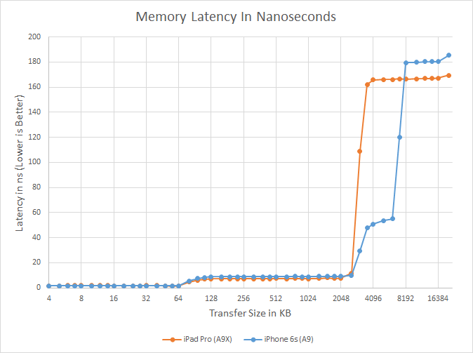
What Chipworks’ die shot now lets us confirm is that this wasn’t a fluke in our tools or the consequence of a change in how Apple’s L3 cache mechanism worked, but rather that there isn’t any L3 cache at all. After introducing the L3 cache with the A7 in 2013, Apple has eliminated it from the A9X entirely. The only cache to be found on A9X are the L1 and L2 caches for the CPU and GPU respectively, along with some even smaller amounts for cache for various other functional blocks.
The big question right now is why Apple would do this. Our traditional wisdom here is that the L3 cache was put in place to service both the CPU and GPU, but especially the GPU. Graphics rendering is a memory bandwidth-intensive operation, and as Apple has consistently been well ahead of many of the other ARM SoC designers in GPU performance, they have been running headlong into the performance limitations imposed by narrow mobile memory interfaces. An L3 cache, in turn, would alleviate some of that memory pressure and keep both CPU and GPU performance up.
One explanation may be that Apple deemed the L3 cache no longer necessary with the A9X’s 128-bit LPDDR4 memory bus; that 51.2GB/sec of bandwidth meant that they no longer needed the cache to avoid GPU stalls. However while the use of LPDDR4 may be a factor, Apple’s ratio of bandwidth-to-GPU cores of roughly 4.26GB/sec-to-1 core is identical to A9’s, which does have an L3 cache. With A9X being a larger A9 in so many ways, this alone isn’t the whole story.
What’s especially curious is that the L3 cache on the A9 wasn’t costing Apple much in the way of space. Chipworks puts the size of A9’s 4MB L3 cache block at a puny ~4.5 mm2, which is just 3% the size of A9X. So although there is a cost to adding L3 cache, unless there are issues we can’t see even with a die shot (e.g. routing), Apple didn’t save much by getting rid of the L3 cache.
Our own Andrei Frumusanu suspects that it may be a power matter, and that Apple was using the L3 cache to save on power-expensive memory operations on the A9. With A9X however, it’s a tablet SoC that doesn’t face the same power restrictions, and as a result doesn’t need a power-saving cache. This would be coupled with the fact that with double the GPU cores, there would be a lot more pressure on just a 4MB cache versus the pressure created by A9, which in turn may drive the need for a larger cache and ultimately an even larger die size.
As it stands there’s no one obvious reason, and it’s likely that all 3 factors – die size, LPDDR4, and power needs – all played a part here, with only those within the halls of One Infinite Loop knowing for sure. However I will add that since Apple has removed the L3 cache, the GPU L2 cache must be sizable. Imagination’s tile based deferred rendering technology needs an on-chip cache to hold tiles in to work on, and while they don’t need an entire frame’s worth of cache (which on iPad Pro would be over 21MB), they do need enough cache to hold a single tile. It’s much harder to estimate GPU L2 cache size from a die shot (especially with Apple’s asymmetrical design), but I wouldn’t be surprised of A9X’s GPU L2 cache is greater than A9’s or A8X’s.
In any case, the fact that A9X lacks an L3 cache doesn’t change the chart-topping performance we’ve been seeing from iPad Pro, but it means that Apple has once more found a way to throw us a new curveball. And closing on that note, we’ll be back in December with our full review of the iPad Pro and a deeper look at A9X’s performance, so be sure to stay tuned for that.
Read More ...
Best Convertible Laptops: Holiday 2015
I break convertibles down into two different segments. The first are those that are a tablet first, and those are defined by having the CPU and other parts in the display section. Keyboards are an add-on on these devices, and they generally are a better tablet experience, with somewhat compromised keyboards and with the heavy tablet section sitting out over the hinge, they do not have as good of a balance when compared to a traditional notebook. The other segment is ones where the keyboard can flip around underneath the display. As a tablet, they are not as good, since the heavy keyboard section stays attached, but as a regular notebook they have the advantage with balance and generally a better typing experience.
We’ve seen some great additions to the lineup for this year, and with Intel’s updated Skylake platform being used by many. Lower cost devices may turn to Intel’s Cherry Trail or Braswell platforms, which are lower performance Atom cores but with a much lower TDP and greater efficiency.
Tablet devices with attachable keyboards
Budget Convertible: ASUS T100HA

ASUS basically invented this class, with the launch of the original T100 back in 2013. For 2015, ASUS is back with a refresh on their 10.1-inch convertible. It is the T100HA, and it’s now powered by Intel’s Cherry Trail with the x5-Z8500 SoC. This is a quad-core 14 nm processor with a 1.44 Ghz base frequency and 2.24 GHz turbo, and since it is Cherry Trail the power requirements are very low, with it having a TDP of just 2 Watts. ASUS offers two models of this, with a 2 GB memory and 32 GB eMMC offering, as well as a 4 GB memory and 64 GB eMMC model. The latter is a great price, at just $279 USD. With 64 GB and Windows 10, space should be fine for basic tasks. ASUS even includes a USB-C connector on the T100HA. The display is decidedly low resolution, at 1280x800, but that is a 16:10 display for those doing the math. The keyboard and trackpad are small, but for the price, it’s hard to beat the T100HA
Mid-Range: Microsoft Surface 3

The Microsoft Surface 3 is the first of the non-pro models from Microsoft to sport an x86 processor, which opens up the entire Windows software ecosystem to Microsoft’s lower cost tablet. The 10.8-inch display is a wonderful 3:2 aspect ratio, with a resolution of 1920x1280. This makes it a much better tablet than the former 16:9 models, especially in portrait mode. The Surface 3 is also powered by Cherry Trail, but in this case the top end x7-Z8700 model. The base clock is 1.6 GHz and boost jumps to 2.4 GHz. The 2-Watt processor does a decent job running Windows 10, but it still can’t hold a candle to Intel’s Core series. Microsoft has bumped the base storage to 64 GB of eMMC, with 2 GB of memory, or you can jump to 4 GB with 128 GB of eMMC. There is micro SD as well if you need to add a bit more storage, and with the latest Windows 10 updates it’s very easy to use the SD for data or even apps. The Surface 3 has a very premium build quality, with a great magnesium finish, and the included kickstand of Surface has three different stops on the new model. It also adds support for Surface pen, and of course the type cover option to transform it into a laptop. It’s not an inexpensive purchase, but the display and build quality are a step ahead of most of the competition.
High-End: Microsoft Surface Pro 4

The latest iteration of the Surface Pro makes some big strides, and distances itself from the competition even further. There have actually been quite a few Surface Pro clones released this year, but it’s going to be a tall task to overcome the incumbent. Pretty much all of the issues with the last generation Surface Pro 3, which was already a great device, have been sorted out with the new model. The processor is now the latest generation Skylake, with options up to the Core i7-6650U with Iris Pro graphics, and if you want fanless, the base model is a Core m3-6Y30. System memory starts at 4 GB, but you can get up to 16 GB on the higher end versions. Storage is now PCIe NVMe with 128 GB as the base offering, and up to a whopping 1 TB is going to be available soon. One issue with the Surface Pro 3 was that it had a tendency to throttle under heavy load, but the new cooling system in the Surface Pro 4 fixes that too. The display in the latest model is a fantastic 267 pixels per inch, with a 3:2 aspect ratio. Even more, the new type cover improves the typing experience immensely, and the larger, smoother, trackpad is now on par with good notebooks. The Surface Pro 4 starts at $899, with prices going way up from there depending on options. It’s not inexpensive, but the Surface Pro 4 delivers.
Notebook first: 360 degree hinge
14-inch with optional NVIDIA Graphics: Lenovo Yoga 700
Lenovo’s Yoga was the original 360-degree hinge laptop, and it adds a lot of functionality over a traditional notebook by being able to couple touch with the hinge. You gain access to not only the tablet mode, but also tend and stand modes. For late 2015, Lenovo has refreshed the lineup and the Yoga 700 makes our list. It’s a 14-inch notebook, but it packs Skylake processors and even an optional NVIDIA GT 940M GPU inside. The display is a reasonable 1920x1080, which of course includes multi-touch. The Yoga 700 loses out on the weight and thickness battle with Lenovo’s higher end models, but it makes up for that in price. The 3.5 lb notebook starts at just $770 with a Core i5-6200U, and for $900 you can get the Core i7-6500U with double the storage (256 GB vs 128 GB on the base) as well as the GT 940M GPU.
Buy the Lenovo Yoga 700 on Lenovo.com
Beautiful aluminum design: HP Spectre x360

HP released their own version of a convertible notebook this year with the release of the HP Spectre x360. They have recently refreshed it to include Skylake processors too. The HP offers great battery life, as well as a beautiful aluminum finish. The trackpad is enormous, with a much wider model than most devices offer. Although we have not had a chance to review the Spectre, I’ve been using one since April and the build quality is top notch. The HP has a great keyboard too, although I’m not a fan of silver keys with white backlighting since they get washed out in any sort of lighting. The base model offers a 1920x1080 display, and you can also get a 2560x1440 model as well. I would likely stick with the 1080p model for battery life reasons, and the base display is quite good. HP doesn’t break the bank either with their nicely crafted convertible. The HP Spectre x360 starts at just $799 with a Core i5-6200U, 8 GB of memory, and 128 GB of storage.
Buy the HP Spectre x360 on HP.com
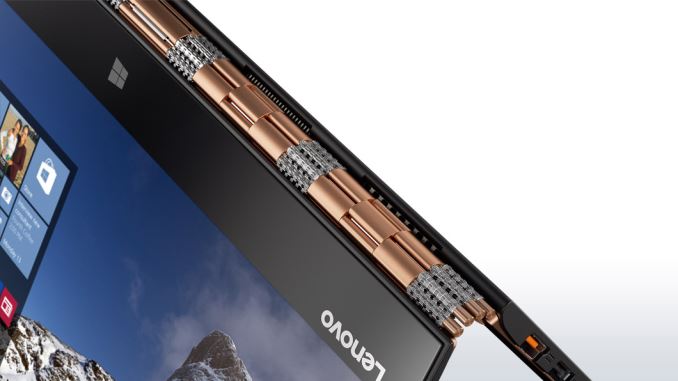
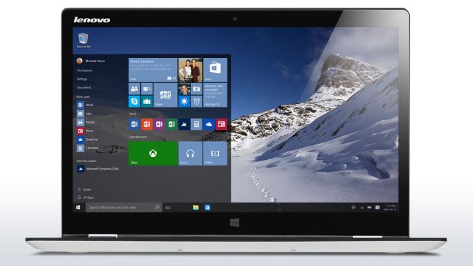
High resolution and amazing hinge: Lenovo Yoga 900

Lenovo has once again revamped their Yoga lineup, and the top end of the consumer lineup is now the Yoga 900. This is a successor to the Yoga 3 Pro, and Lenovo looks to fix some of the ailments of that model. The Yoga 3 Pro went for thin and light over pretty much anything, and it did it by using Core M. For the Yoga 900, Lenovo has made it slightly thicker, but by doing so they have been able to move back to the 15-Watt Core processors. They have also increased battery capacity, which is now an impressive 66 Wh. The display is the same 3200x1800 IPS panel, for good and bad. I really hope that Lenovo moves away from this Samsung RGBW Pentile display for future models, since there are plenty of better choices out there now. But still, the overall laptop keeps its thin and light design, along with the beautiful watchband hinge. The 1.3 kg (2.8 lb) convertible is just 14.9 mm (0.59”) thick. You also get USB-C with video out, and the base specifications have gotten a bump. Storage now starts at 256 GB, and can move to 512 GB, and RAM starts at 8 GB and they also offer a 16 GB model. The new Yoga 900 starts at $1200, and goes up to $1400 with 16 GB of memory and 512 GB of storage.
Buy the Lenovo Yoga 900 on Lenovo.com
This wraps up our look at laptops for 2015. It has been a great year for notebooks, with some amazing new models in all categories.
Read More ...
The Microsoft Band 2 Review
At the end of October in 2014, Microsoft surprisingly released a late night press release about a new device they were launching. It was the Microsoft Band, which is a fitness wearable that was a key component of their Microsoft Health service. It was their first real wearable, and it was packed with sensors to track everything from your heart rate to your sleep quality. At the Microsoft devices event in NYC on October 6th, Microsoft announced an updated version of the Band, known as Band 2. Its goal is to provide even more health insights, while being more comfortable and stylish than the original Band.
Read More ...
Retiree Sues Apple For $7,500 for Wiping Honeymoon Photos From His iPhone
"15 years worth of contacts" were also lost
Read More ...
Available Tags:AMD , GPU , Microsoft , Apple , His , iPhone ,
No comments:
Post a Comment