
A Few Notes on Intel’s Knights Landing and MCDRAM Modes from SC15
As such, I attended a tutorial session here at SuperComputing15 on the MCDRAM (Multi-Channel DRAM) used in Intel’s 2nd generation Xeon Phi, code named Knights Landing (KNL). Specifically the talk focused on the analysis methods and tools, and it went into greater depth as to how the implementation works.
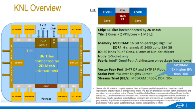
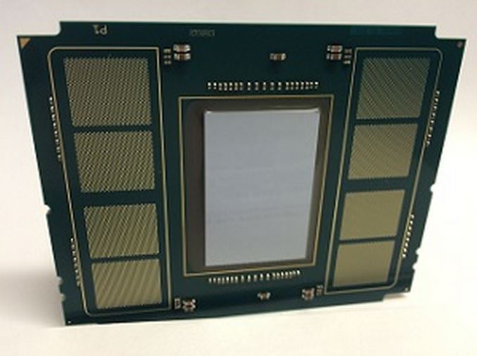
Some of the KNL overview we have seen before – the 72 Silvermont-based cores running at ~1.3 GHz are split into tiles with two cores per tile, two VPUs (Vector Processing Units, AVX-512) per core and each tile shares 1MB of L2 cache for a total of 36MB of L2 across the design. Rather than the ring topology we see in the standard processor designs from Intel, they are arranged in a mesh topology using an interconnected fabric (which seems to be sets of rings anyway). Despite the 6x7 nature of the image above, shots of the package have had some question that the layout is more akin to a 4x9, although this is unconfirmed.
The big paradigm shifts are everywhere. KNL can be used as the main processor in a computer, running an OS on top of all the cores, or as a co-processor similar to former Xeon Phi silicon – but as noted above in the slide there is no version of QPI for 2P/4P systems. There are a total of 36 PCI 3.0 lanes though, for PCIe co-processors, as well as onboard Omni-Path control for network interconnects. The cores are 14nm versions of Silvermont, rather than 22nm P54C, with claims that the out-of-order performance is vastly improved. The die has a total of 10 memory controllers – two for DDR4 controllers (supporting three channels each), and then eight for MCDRAM.
Each of these high-bandwidth controllers link out to a the on-package MCDRAM (we believe stacked 20nm Micron Planar DRAM) through an on-package interposer, offering 400+ GB/s of bandwidth when all the memory is used in parallel. This sounds similar to AMD’s Fiji platform, which offers 4GB of memory over four HBM (high bandwidth memory) packages, but Intel is prepared to offer 16GB of MCDRAM ‘at launch’. The fact that Intel says at launch could be suggested that there are plans to move into higher capacities in the future.
As the diagram stands, the MCDRAM and the regular DDR4 (up to six channels of 386GB of DDR4-2400) are wholly separate, indicating a bi-memory model. This stands at the heart at which developers will have to contend with, should they wish to extract performance from the part.
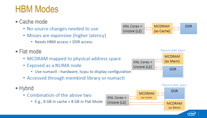
The KNL memory can work in three modes, which are determined by the BIOS at POST time and thus require a reboot to switch between them.
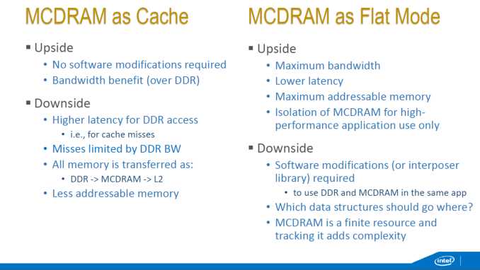
The first mode is a cache mode, where nothing is needed to be changed in the code. The OS will organize the data to use the MCDRAM first similar to an L3 cache, then the DDR4 as another level of memory. Intel was coy onto the nature of the cache (victim cache, writeback, cache coherency), but as it is used by default it might offer some performance benefit up to 16GB data sizes. The downside here is when the MCDRAM experiences a cache miss – because of the memory controllers the cache miss has to travel back into the die and then go search out into DDR for the relevant memory. This means that an MCDRAM cache miss is more expensive than a simple read out to DDR.
The second mode is ‘Flat Mode’, allowing the MCDRAM to have a physical addressable space which allows the programmer to migrate data structures in and out of the MCDRAM. This can be useful to keep large structures in DDR4 and smaller structures in MCDRAM. We were told that this mode can also be simulated by developers who do not have hardware in hand yet in a dual CPU Xeon system if each CPU is classified as a NUMA node, and Node 0 is pure CPU and Node 1 is for memory only. The downside of the flat mode means that the developer has to maintain and keep track of what data goes where, increasing software design and maintenance costs.
The final mode is a hybrid mode, giving a mix of the two.
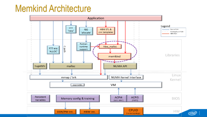
In flat mode, there are separate ways to access the high performance memory – either as a pure NUMA node (only applicable if the whole program can fit in MCDRAM), using direct OS system calls (not recommended) or through the Memkind libraries which implements a series of library calls. There is also an interposer library over Memkind available called AutoHBW which simplifies some of the commands at the expense of fine control. Under Memkind/AutoHBW, data structures aimed at MCDRAM have their own commands in order to be generated in MCDRAM.
Intel’s VTune utilities will be enabled with KNL from VTune Amplifier XE2016.
There was some talk regarding Intel’s upcoming 3D XPoint which offers another layer of memory but this time in a non-volatile format. We were told to expect 3D XPoint to become a part of future Xeon Phi designs, along with multi-level memory management (potentially three: MCDRAM, DDR, XPoint), although the exact nature of how many levels of memory, or what types and how to use them, is still undecided. What we do know about the future is that the 3rd generation of Xeon Phi will be built on 10nm and named Knights Hill, featuring 2nd generation Omni-Path host fabric.
Source: Intel, SC15
Read More ...
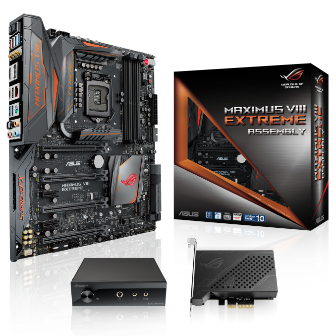
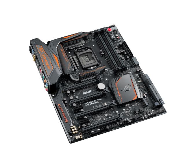
ASUS Launches Maximus VIII Extreme/Assembly for Skylake, includes 10G Ethernet Card
10G Ethernet, or at least 10GBase-T, the standard which uses the common RJ-45 Ethernet cables that run through most enthusiast homes, workplaces and hotels, has struggled to get into mainstream computing for various reasons. We saw the ASRock X99 WS-E/10G motherboard be introduced late last year with an onboard Intel X540-T2 controller, but the motherboard was expensive as a result and it was only even an integrated part on the high-end desktop. For everyone else, using a PCIe card with 10GBase-T connectors was the only way to do so, but these were again quite expensive (I spent $760 on two a few months back) and ran warm. Most of these cards are OEM only, although the generic retailers can sometimes stock them.
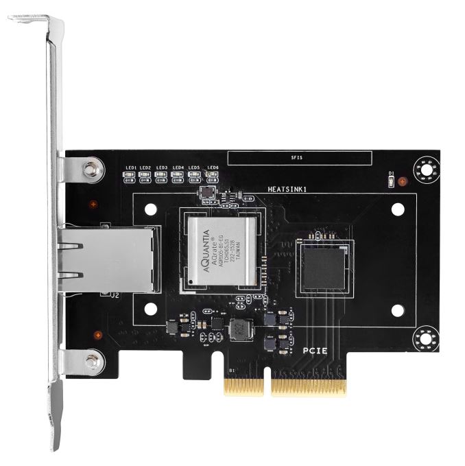
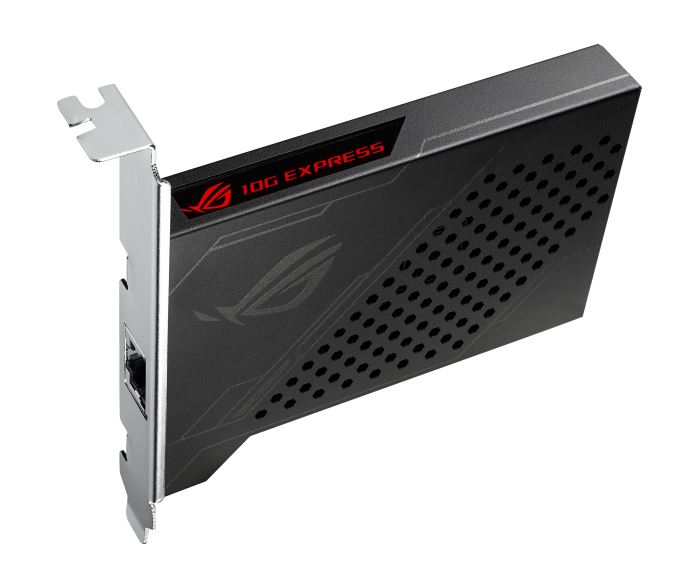
The 10G card ASUS is bundling with the new variant of the Maximus VIII Extreme is one based on Aquantia and Tehuti Networks. Don’t worry, I hadn’t heard of them before either – Ganesh did though with one of them. The card is a PCIe 2.0 x4 card that will be verified in all the PCIe x4 and up slots on the motherboard (including from the chipset, so it won’t take up graphics lanes), but is also capable of 2.5G and 5G speeds should routers for those ever become available. The package also supports standard gigabit Ethernet, with the card being a larger version of Tahuti Network’s own that we found here, and with ROG branding.
There is an argument that 10GBase-T isn’t really a home networking type of arrangement – the switches still cost a minimum of $750 for Netgear’s XS708E. There’s also no point having one system with 10G if no others on your network do either. The counter position is that this motherboard package is north of $500 anyway, so it will only be purchased by enthusiasts or prosumers (or even small/medium businesses that already own a 10G capable Xeon-D NAS or backbone, although they might only just want the card). We are told that there are no plans to sell the card individually either at this point, with the bundle coming to the US at least sometime in the next few weeks.
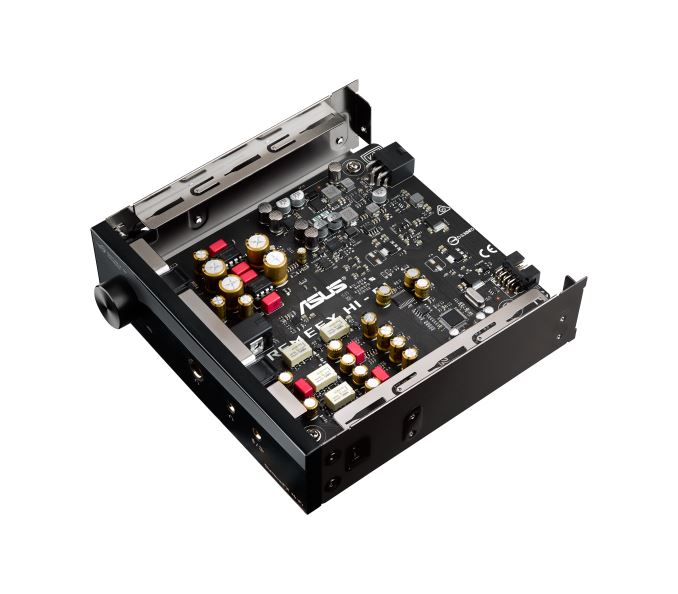
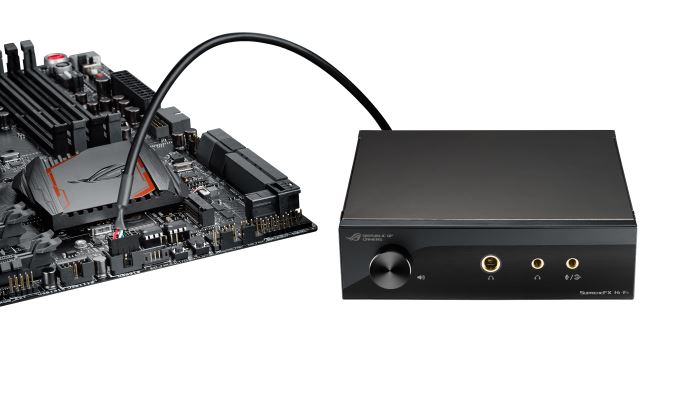
Networking aside, the Maximus VIII Extreme is still the same board with U.2 capability, 3T3R 802.11ac wireless, USB 3.1 via both the Intel Alpine Ridge controller as well as ASMedia USB 3.1 controllers, enhanced audio via the SupremeFX brand and overclocking functionality. The SupremeFX Hi-Fi bundled front panel is the additional USB style DAC front panel box, featuring a headphone amp based on an ESS ES9018K2M DAC, dual TI op-amps and an output of over 6V RMS to high impedance headphones.
We have a review inbound for the Maximus VIII Extreme (it’s pretty much tested, need to finish up then write), but it would be interesting to see how the 10G card performs compared to other solutions. No pricing as of yet until the US specific press release hits.


Source: ASUS
Read More ...
Intel @ SC15: Launching Xeon Phi “Knights Landing” & Omni-Path Architecture
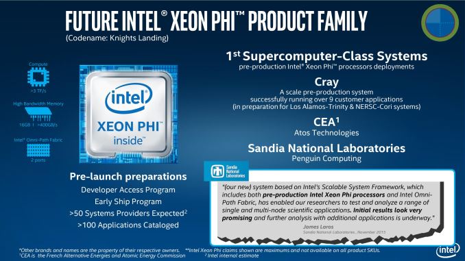
The 14nm successor to Knights Corner (1st gen Xeon Phi), Knights Landing implements AVX-512, Multi-Channel DRAM (MCDRAM), and a new CPU core based on Intel’s Silvermont architecture. Knights Landing is now shipping to Intel’s first customers and developers as part of their early ship program, and pre-production systems for demonstrating supercomputer designs are up and running. Knights Landing is ultimately ramping up for general availability in Q1 of 2016, at which point I expect we’ll also get the final SKU specifications from Intel.
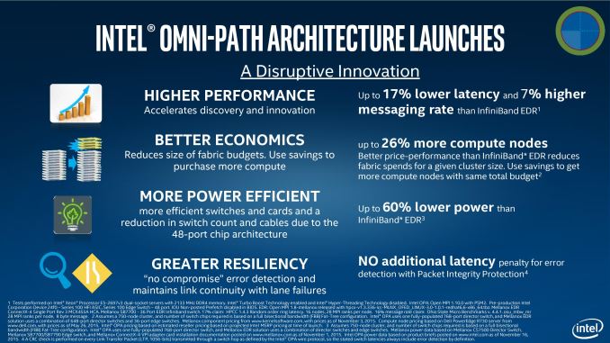
Meanwhile Knights Landing’s partner in processing, Intel’s Omni-Path Architecture, is formally launching at SC15. Intel’s own take on a high bandwidth low-latency interconnect for HPC, Omni-Path marks Intel’s greatest efforts yet to diverge from InfiniBand and go their own way in the market for interconnect fabrics. We covered Omni-Path a bit earlier this year at Intel’s IDF15 conference, so there aren’t any new technical details to touch upon, however Intel is now throwing out their official performance figures for Omni-Path versus InfiniBand EDR, including the power savings of their larger 48-port switch capabilities.
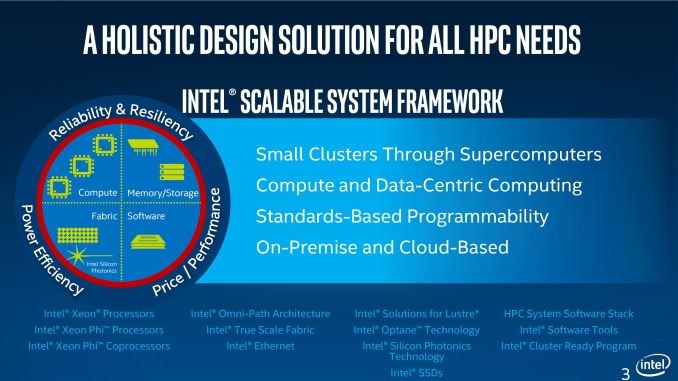
Ultimately Knights Landing and Omni-Patch Architecture are part of Intel’s larger efforts to build a whole ecosystem, which they’ve been calling the System Scalable Framework. Along with the aforementioned hardware, Intel will be showing off some of the latest software developments for the SSF on the SC15 show floor this week.


Read More ...
NVIDIA @ SC15: US NOAA to Build Tesla Weather Research Cluster
Along with touting the number of major HPC applications that are now GPU accelerated and the performance impact of that process, NVIDIA’s other major focus at SC15 is to announce their next US government contract win. This time the National Oceanic and Atmospheric Administration (NOAA) is tapping NVIDIA to build a next-gen research cluster. The system, which doesn’t currently have a name, is on a smaller scale than the likes of Summit & Sierra, and will be comprised of 760 GPUs. The cluster will be operational next year, and giving the timing and the wording as a “next-generation” cluster, it’s reasonable to assume that this will be Pascal powered.

The purpose of the NOAA cluster will be to develop a higher resolution and ultimately more accurate global forecast model. To throw some weather geekery on top of some technology geekery, in recent years the accuracy of the NOAA’s principle global forecast model, the GFS, has fallen behind the accuracy of other competing models such as the European ECMWF. The most famous case of this difference in accuracy is in 2012, when the GFS initially failed to predict that Hurricane Sandy would hit the US, something the ECMWF correctly predicted. As a result there has been a renewed drive towards improving the US models and catching up with the ECMWF, which in turn is what the NOAA’s research cluster will be used to develop.
Weather forecasting has in turn been a focus of GPU HPC work for a couple of years now – NVIDIA already has Tesla wins for supercomputers that are being used for weather research – but this is the first NOAA contact for the company. Somewhat fittingly, this comes as the NOAA’s Geophysical Fluid Dynamics Laboratory already runs their simulations out of Oak Ridge, home of course to Titan.


Read More ...
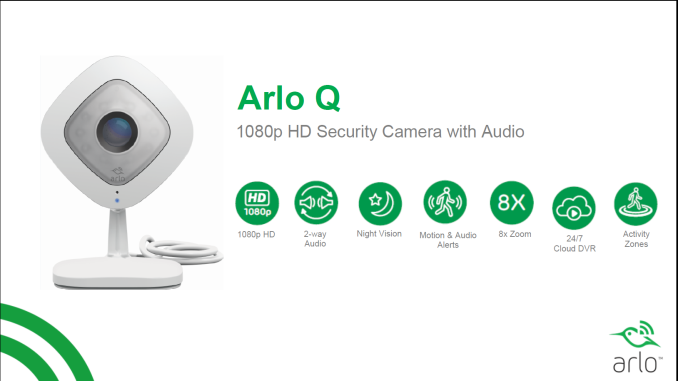
Netgear Expands Smart Home Lineup with Arlo Q IP Camera
Netgear had an interesting slide to share with respect to the market share status of the Arlo.

Within 6 months of introduction, the Arlo managed to climb up to the top of the charts with a 20% share (also helped by Dropcam making a slow transition to the new Nest Cam model). This shows that there is a tremendous market potential for battery-operated IP cameras (something we had not foreseen when the Arlo Wire-Free was launched).
IP cameras such as Nest Cam (Dropcam) and D-Link's myriad offerings also enjoy success in the market because they address use-cases for which the Arlo Wire-Free isn't suitable:
- Continuous recording for long events of interest
- Ability to have 2-way live communication via built-in speakers / microphones
- Higher resolution for better details in captured video
- Analytics capabilities - intelligent detection and ability to set up activity zones
Netgear is introducing the Arlo Q today to address some of these issues. It is intended to be complementary to the Arlo Wire-Free model that will be continue to be sold concurrently.
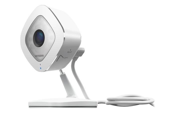
The hardware aspects of the Arlo Q are summarized below:
- Up to 1080p30 video recording (depending on bandwidth availability)
- 4MP sensor resolution
- 15' night vision with 850nm IR
- Dual-band N600 Wi-Fi
- Integrated speaker and microphone for 2-way audio
- 130 degree field-of-view
Other aspects include:
- Detection for recording using activity zones and/or audio triggers
- 7 days of free cloud video recording for the lifetime of the device
- Mobile notifications
- iOS and Android apps as well as web browser support for video stream viewing
- Provision for flexible placement (magnetic mounting / wall-mounting brackets / desktop placement)
- Provision for scheduling recordings (armed / disarmed for motion / audio triggers, scheduling as well as geofencing capabilities)
Compared to the Nest Cam (which supports only live viewing of the video stream for free, but requires a subscription for cloud recording), Netgear provides seven days of rolling cloud recordings for free (based on motion or audio events). Continuous Video Recording (CVR) is available either on a 14-day or 30-day rolling window plan with the service rates varying depending on the duration as well as the number of cameras in the plan. Note that a subscription is not an essential requirement to take good advantage of most of the capabilities of the Arlo Q.

We have generally been wary of recommending smart home products that rely purely on the cloud for operation. While the Arlo lineup is currently heavily dependent on the cloud (just like the Nest Cam), Netgear did assure us that they had no qualms in enabling local recording of the video stream (either to storage attached to the Arlo hub or a ReadyNAS unit in the same local network) sometime in the future. Apparently, the main concern is the security of the video stream. Given the 7-day free recording feature, it is clear that Netgear is not relying entirely on the CVR feature to drive the revenue up for the product (which is good for the consumers).
Netgear also indicated that the Arlo Q and the current Nest Cam both use SoCs from the same vendor, with the one used in the the Arlo Q being the next-generation version of the one in the Nest Cam. Given this information, it is likely that the video quality as well as the streaming bitrate will be similar to (or better than) the one from the Nest Cam. It is great that the market will get a more consumer-friendly alternative to the Nest Cam, though we would be more enthusiastic if Netgear had the local recording capabilities ready at launch time. The Arlo Q (VMC3040) will be available in December 2015 and have a MSRP of $220.
Read More ...
The Corsair H80i GT and H100i GTX AIO Coolers Review
Today we are having a look at the upgraded 120 mm AIO liquid coolers from Corsair, the single slot H80i GT and the dual slot H100i GTX. Both come with two high pressure 120 mm fans, are based on the same core design and feature RGB lighting and Corsair Link support. In this review we also examine their performance, especially in relation to the vanilla H80i and H100i versions.
Read More ...
AMD @ SC15: Boltzmann Initiative Announced - C++ and CUDA Compilers for AMD GPUs
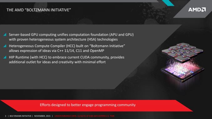
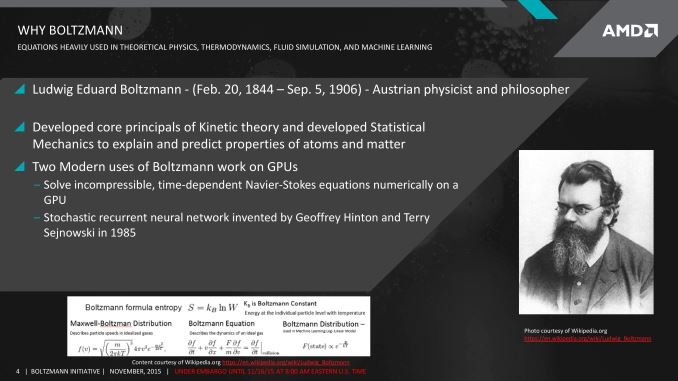
So what has AMD so excited for SC15? In short the company is about to embark on a massive overhaul of their HPC software plans. Dubbed the Boltzmann Initiative – after father of statistical mechanics Ludwig Boltzmann – AMD will be undertaking a much needed redevelopment effort of their HPC software ecosystem in order to close the gap with NVIDIA and offer an environment competitive (and compatible!) with CUDA. So with that in mind, let’s jump right in.
Headless Linux & HSA-based GPU Environment
Perhaps the cornerstone of the Boltzmann Initiative is with AMD’s drivers, which are being improved and overhauled to support AMD’s other plans. The company will be building a dedicated 64-bit Linux driver specifically for headless operation under Linux. It’s only been in the last year that AMD has really focused on headless Linux operation – prior to that headless OpenCL execution was a bit of a hack – and with the new driver AMD completes what they’ve started.

But more importantly than that, the headless Linux driver will be implementing an HSA extended environment, which will bring with it many of the advantages of the Heterogeneous System Architecture to AMD’s FirePro discrete GPUs. This environment, which AMD is calling HSA+, builds off of the formal HSA standard by adding extensions specifically to support HSA with discrete GPUs. The extensions themselves are going to be non-standard – the HSA Foundation has been focused on truly integrated devices ala APUs, and it doesn’t sound like these extensions will be accepted upstream into mainstream HSA any time soon – but AMD will be releasing the extensions as an open source project in the future.
The purpose of extending HSA to dGPUs, besides meeting earlier promises, is to bring as many of the benefits of the HSA execution model to dGPUs as is practical. For AMD this means being able to put HSA CPUs and dGPUs into a single unified address space – closing a gap with NVIDIA since CUDA 6 – which can significantly simplify programming for applications which are actively executing work on both the CPU and the GPU. Using the HSA model along with this driver also allows AMD to address other needs such as bringing down dispatch latency and improving support/performance for large clusters where fabrics such as InfiniBand are being used to link together the nodes in a cluster. Combined with the basic abilities of the new driver, AMD is in essence laying some much-needed groundwork to offer a cluster feature set more on-par with the competition.
Heterogeneous Compute Compiler – Diverging From OpenCL, Going C++
The second part of the Boltzmann Imitative is AMD’s new compiler for HPC, the Heterogeneous Compute Compiler. Built on top of work the company has already done for their HSA compiler, the HCC will be the first of AMD’s two efforts to address the programming needs of the HPC user base, who by and large has passed on AMD’s GPUs in part for a lackluster HPC software environment.
As a bit of background here before going any further, one of the earliest advantages for NVIDIA and CUDA was supporting C++ and other high-level programming languages at a time when OpenCL could only support a C-like syntax, and programming for OpenCL was decidedly at a lower level. AMD meanwhile continued to back OpenCL, in part in order to support an open ecosystem, and while OpenCL made great strides with the provisional release of OpenCL 2.1 and OpenCL C++ kernel language this year, in a sense the damage has been done. OpenCL sees minimal use in the HPC space, and further complicating matters is the fact that not all of the major vendors support OpenCL 2.x. AMD for their part is polite enough not to name names, but at this point the laggard is well known to be NVIDIA, who only supports up to OpenCL 1.2 (and seems to be in no rush to support anything newer).

As a result of these developments AMD is altering their software strategy, as it’s clear that the company can no longer just bank on OpenCL for their HPC software API needs. I hesitate to say that AMD is backing away from OpenCL at all, as in our briefings AMD made it clear that they intend to continue to support OpenCL, and based on their attitude and presentation this doesn’t appear to be a hollow corporate boilerplate promise in order to avoid rocking the boat. But there’s a realization that even if OpenCL delivers everything AMD ever wanted, it’s hard to leverage OpenCL when support for the API is fragmented and when aspects of OpenCL C++ are still too low level, so AMD will simultaneously be working on their own API and environment.
This environment will be built around the Heterogeneous Compute Compiler. In some ways AMD’s answer to CUDA, the HCC is a single C/C++/OpenMP compiler for both the CPU and the GPU. Like so many recent compiler projects, AMD will be leveraging parts of Clang and LLVM to handle the compilation, along with portions of HSA as previously described to serve as the runtime environment.
The purpose of the HCC will be to allow developers to write CPU and/or GPU code using a single compiler, in a single language, inside a single source file. The end result is something that resembles Microsoft’s C++ AMP, with developers simply making parallel calls within a C++ program as they see fit. Perhaps most importantly for AMD and their prospective HPC audience, HCC means that a separate source file for GPU kernels is not needed, a limitation that continues to exist right up to OpenCL++.
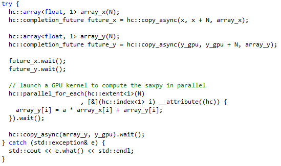
Overall HCC will expose parallelism in two ways. The first of which is through explicit syntax for parallel operations, ala-C++ AMP, with developers calling parallel-capable functions such as parallel_for_each to explicitly setup segments of code that can be run in parallel and how that interacts with the rest of the program, with this functionality built around C++ lambda code. The second method, at an even higher level, will be to leverage the forthcoming Parallel STL (Standard Template Library), which is slated to come with C++ 17. The Parallel STIL will contain a number of parallelized standard functions for GPU/accelerator execution, making things even simpler for developers as they no longer need to explicitly account for and control certain aspects of parallel execution, and can use the STL functions as a base for modification/extension.
Ultimately HCC is intended to modernize GPU programming for AMD GPUs and to bring some much-desired features to the environment. Along with the immediate addition of basic parallelism and standard parallel functions, the HCC will also include some other features specifically for improving performance on GPUs and other accelerators. This includes support for pre-fetching data, asynchronous compute kernels, and even scratchpad memories (i.e. the AMD LDS Local Data Share). Between these features, AMD is hopeful that they can offer the kind of programming environment that HPC users have wanted, an environment that is more welcoming to new HPC programmers, and an environment that is more welcoming to seasoned CUDA programmers as well.
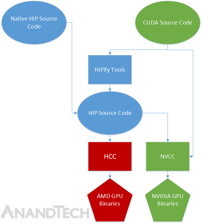
Heterogeneous-compute Interface for Portability (HIP) – CUDA Compilation For AMD GPUs
Last but certainly not least in the Boltzmann Initiative is AMD’s effort to fully extend a bridge into the world of CUDA developers. With HCC to bring AMD’s programming environment more on par with what CUDA developers expect, AMD realizes that just being as good as NVIDIA won’t always be good enough, that developers accustomed to the syntax of CUDA won’t want to change, and that CUDA won’t be going anywhere anytime soon. The solution to that problem is the Heterogeneous-compute Interface for Portability, otherwise known as HIP, which gives CUDA developers the tools they need to easily move over to AMD GPUs.

Through HIP AMD will bridge the gap between HCC and CUDA by giving developers a CUDA-like syntax – the various HIP API commands – allowing developers to program for AMD GPUs in a CUDA-like fashion. Meanwhile HIP will also including a toolset (the HIPify Tools) that further simplifies porting by automatically converting CUDA code to HIP code. And finally, once code is HIP – be it natively written that way or converted – it can then be compiled to either NVIDIA or AMD GPUs through NVCC (using a HIP header file to add HIP support) or HCC respectively.
To be clear here, HIP is not a means for AMD GPUs to run compiled CUDA programs. CUDA is and remains an NVIDIA technology. But HIP is the means for source-to-source translation, so that developers will have a far easier time targeting AMD GPUs. Given that the HPC market is one where developers are typically writing all of their own code here anyhow and tweaking it for the specific architecture it’s meant to run on, a source-to-source translation covers most of AMD’s needs right there, and retains AMD’s ability to compile CUDA code from a high level where they can better optimize that code for their GPUs.
Now there are some unknowns here, including whether AMD can keep HIP up to date with CUDA feature additions, but more importantly there’s a question of just what NVIDIA’s reaction will be. CUDA is NVIDIA’s, through and through, and it does make one wonder whether NVIDIA would try to sue AMD for implementing the CUDA API without NVIDIA’s permission, particularly in light of the latest developments in the Oracle vs. Google case on the Java API. AMD for their part has had their legal team look at the issue extensively and doesn’t believe they’re at risk – pointing in part to Google’s own efforts to bring CUDA support to LLVM with GPUCC – though I suspect AMD’s efforts are a bit more inflammatory given the direct competition. Ultimately it’s a matter that will be handled by AMD and NVIDIA only if it comes to it, but it’s something that does need to be pointed out.
Otherwise by creating HIP AMD is solving one of the biggest issues that has hindered the company’s HPC efforts since CUDA gained traction, which is the fact that they can’t run CUDA. A compatibility layer against a proprietary API is never the perfect solution – AMD would certainly be happier if everyone could and did program in standard C++ – but there is a sizable user base that has grown up on CUDA and is at this point entrenched with it. And simply put AMD needs to have CUDA compatibility if they wish to wrest HPC GPU market share away from NVIDIA.

Wrapping things up then, with the Boltzmann Initiative AMD is taking an important and very much necessary step to redefine themselves in the HPC space. By providing an improved driver layer for Linux supporting headless operation and a unified memory space, with a compiler for direct, single source C++ compilation on top of that, and a CUDA compatibility layer to reach the established CUDA user base, AMD Is finally getting far more aggressive on the HPC side of matters, and making the moves that many have argued they have needed to make for quite some time. At this point AMD needs to deliver on their roadmap and to ensure they deliver quality tools in the process, and even then NVIDIA earned their place in the HPC space through good products and will not be easily dislodged – CUDA came at exactly the time when developers needed it – but for AMD if they can execute on Boltzmann it will be the first time in half a decade they would have a fighting chance at tapping into the lucrative and profitable HPC market.


Read More ...
IBM & Xilinx @ SC15: Collaborating For Better POWER/FPGA System Integration

For SC15 announcements we’ll start things off with IBM. At the show, Big Blue is announcing that they are forming a strategic partnership with FPGA maker Xilinx to improve the use of FPGAs in POWER-based systems, with a focus on improving HPC workload performance ultimately driving towards greater integration between the two categories of processors.
The increasing integration of FPGAs has been a hot topic over the last few years, as the pace of CPU performance growth has begun to slow and HPC vendors have increasingly turned towards specialty accelerators in order to further improve performance while also ramping up power efficiency as well. FPGAs in turn offer a lot of flexibility due to their programmability, and as a result offer a class of processor that is neither a CPU nor a massively parallel process like a GPU. Consequently there is an increasing bet on FPGAs becoming the 3rd pillar of HPC, sitting alongside CPUs and GPUs to cover what the others cannot. IBM’s announcement comes about half a year after Intel’s announcement that they are purchasing FPGA maker Altera, setting the stage for IBM and others to further develop their own FPGA partnerships.
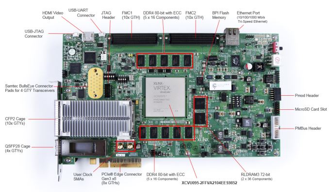
Xilinx Virtex UltraScale FPGA VCU108
Meanwhile thanks to POWER’s CAPI interface, it has already been possible to pair up FPGAs with POWER processors, so today’s announcement is less about technology and more about forming alliances and putting that technology to good use. Of particular note from IBM’s press release:
As part of the IBM and Xilinx strategic collaboration, IBM Systems Group developers will create solution stacks for POWER-based servers, storage and middleware systems with Xilinx FPGA accelerators for data center architectures such as OpenStack, Docker, and Spark. IBM will also develop and qualify Xilinx accelerator boards into IBM Power Systems servers. Xilinx is developing and will release POWER-based versions of its leading software defined SDAccel™ Development Environment and libraries for the OpenPOWER developer community.
That IBM is entering into this agreement with the intention of selling Power Servers with Xilinx FPGAs is probably the most important part of this announcement. This essentially elevates Xilinx from a third party to a second party in the POWER ecosystem, as it’s still IBM that leads the way on POWER servers. This will of course eventually go head-to-head with systems based around Intel’s Xeon family, and their own plans for heterogeneous systems involving FPGAs.
Finally, the larger OpenPOWER community will see some gains as well. Along with the technology IBM shares and the software that will be made available to the OpenPOWER community under this collaboration, Xilinx is now a top-level Platinum member of the OpenPOWER foundation and will have a seat on the board of directors. It’s interesting to note that already Altera sits on this level as well, though with the Intel purchase it’s reasonable to assume that in time Xilinx will replace Altera as the favored, Platinum level FPGA after Intel integrates their purchase.
Read More ...
OnePlus One, OnePlus 2 Will Receive Android Marshmallow in Q1 2016
The road to Android 6.0 is a slow one, but at least OnePlus has committed to a quasi-definitive update schedule
Read More ...
Available Tags:ASUS , Intel , Xeon , NVIDIA , GTX , AMD , C++ , CUDA , AMD , IBM , Android ,
No comments:
Post a Comment