
Podcast 34: IDF Special! Interview with Dr Genevieve Bell, Intel Fellow
Intel’s Developer Forum is an annual event in San Francisco focusing on how Intel attempts to enable product design and by extension, experience. Part of that is along the technical route, covering developments in Intel’s latest technologies in both software and hardware and how to use them best. The other side of the coin is more towards positioning Intel for future development, especially when it comes to IoT, homebrew and more focal applications.
Due to some chance meetings (such as randomly bumping into each other after 9pm near the show floor), we were able to secure some time to interview Dr Genevieve Bell, Intel Fellow, resident anthropologist and Vice President of Intel’s Strategy Office.
It might seem odd for a company like Intel to hire an anthropologist, but Dr Bell has been examining the intersection of technology and human interaction with Intel for almost 16 years, including how computational assistants develop a personality, or are given a gender, to where that data is shared and used and what unique joys and frustrations can arise from the different perception of various aspects of technology based on the users’ environment.
Dr Bell presented a keynote talk at IDF focusing on the maker community currently revolving around Intel, which included examples of historic inventors (Curie, Edison) that could have been considered the makers of their time to the present day with an appearance by Dale Dougherty, the publisher behind Maker magazine and numerous maker events/hackathons around the US and worldwide. As a result, during our time with Dr Bell, we focused on that intersection of makers and the maker community, the altruistic intentions of the designers competing with corporate interests in this space and how the perception of the maker community is currently in a large state of flux from both the perspective of end-users and regulatory insights. Someone also had to bring up the recent cricket scoreline as well, in classic Aussie vs Brit style.
Unfortunately IDF was being dismantled around us after the 16 minute mark, so there is some background noise.
The AnandTech Podcast - Episode 34
Featuring
- Dr Ian Cutress, Host, Senior Editor (@IanCutress)
- Dr Genevieve Bell, Special Guest, Senior Anthropologist and VP of the Corporate Strategy Group at Intel (@FeralData)
iTunes
RSS - mp3, m4a
Direct Links - mp3, m4a
Total Time: 20m 39s
Many thanks to Dr Bell for her time – having been following her online thoughts for a time and finally getting a chance to sit and talk was an almost overwhelming experience. I subsequently forgot most of the questions I had mentally stored, perhaps dwelling on a couple of points with long winded questioning. I promise I’ll be better prepared next time!
Read More ...
The Windows 10 Review: The Old & New Face of Windows
Let’s flash back to 2012. About three years ago, Windows 8, the last major release of Microsoft’s ubiquitous operating system, was released to manufacturers. This was to be Microsoft’s most ambitious release yet. Traditional PC sales were in decline, and more personal devices such as the iPad tablet were poised to end the dominant PC platform. Microsoft’s response to this was to change Windows more than in any previous release, in a bid to make it usable with the tablet form factor. Windows 8 launched in October 2012 to much fanfare, but did not help the struggling PC market recover. Windows 10 is here to fix what ailed Windows 8, with a goal of driving adoption from all older versions with a combination of returning features, new features, and a great set of improvements.
Read More ...
Microsoft Makes Cortana For Android Available As A Public Beta
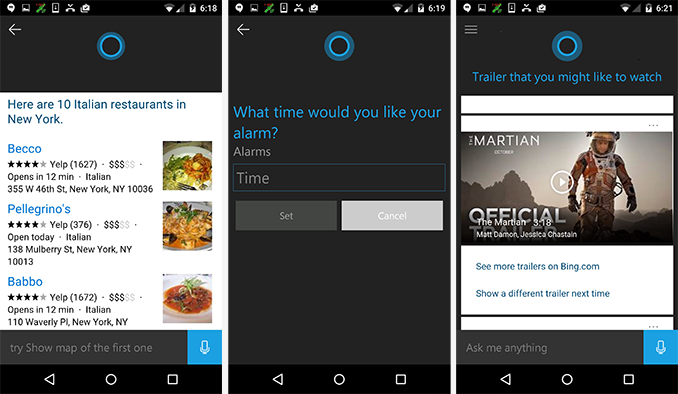
Earlier this year Microsoft announced that their digital assistant Cortana would be making its way to iOS and Android in addition to its launch on Windows Phone and Windows 10. Today Microsoft opened the public beta for Cortana on Android, allowing users to use the same digital assistant on their Android smartphones and tablets as the one on their Windows 10 computers
Because of Android's ability to choose what applications are used for certain tasks, users can alter the long press of their device's home button to trigger Cortana instead of Google Now. As of right now, Cortana on Android has a similar interface and functionality to its Windows counterpart, but at this point in the beta there's no way to use Cortana to toggle settings, launch apps, or to activate Cortana itself by saying "Hey Cortana."
Users interested in trying the public beta for Cortana on Android can use this link to become a beta tester.
Read More ...
Qualcomm Details Hexagon 680 DSP in Snapdragon 820: Accelerated Imaging
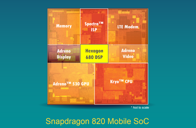
Although we tend not to focus too much on the tertiary aspects of a SoC, they are often important to enabling many aspects of the user experience. DSPs are important for a number of unique applications such as voice processing, audio processing, and other input processing applications. Before we get into the meat of the article though it's important to note that the above image is not a die shot or an actual block diagram, but is very roughly approximating the relative size of each component in the SoC.
Today at Hot Chips, Qualcomm elected to reveal a number of details about their Hexagon 680 DSP, which will ship in the Snapdragon 820. Those that have followed our coverage regarding the Snapdragon 820 ISP features will probably be able to guess that a number of features on the Snapdragon 820 Spectra ISP are enabled through the use of this newer DSP.
For those that are unfamiliar with DSPs, the basic idea behind DSPs is that they are a sort of in-between point in architecture design between highly efficient fixed function hardware (think: video decoders) and highly flexible CPUs. DSPs are programmable, but are rigid in design and are designed to do a limited number of tasks well, making them efficient at those tasks relative to a CPU, but more flexible than fixed function hardware. These design goals are typically manifested in DSPs as in-order architectures, which means that there's much less power and area dedicated on silicon to parallelize code on the fly. This means that while a DSP can do a number of workloads that would otherwise be impossible on a completely fixed-function block, you wouldn't want to try and use one to replace a CPU. It's important to emphasize that DSPs are generally more focused on instruction-level parallelism (single core performance) rather than thread-level parallelism (multi-core performance), so you won't see hundreds/thousands of "cores" in a DSP like you would in a GPU architecture like Maxwell.
Consequently the architecture of DSPs like the Hexagon 680 are relatively alien compared to standard CPUs, as optimization is everything in the applications where DSPs make sense. For example, DSP instruction sets are often VLIW (very long instruction word), in which multiple execution units are driven in parallel with a single instruction. Certain arithmetic operations are also highly accelerated with special instructions in order to enable key algorithms for signal processing such as Fast Fourier Transform (FFT).
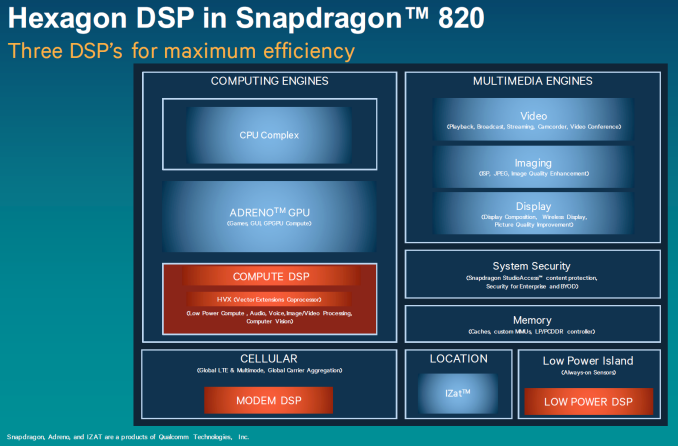
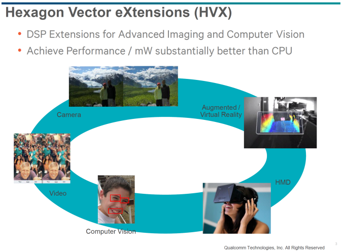
In the case of the Hexagon 680, one of the key features Qualcomm is focusing on for this launch are Hexagon Vector Extensions (HVX). HVX is designed to handle significant compute workloads for image processing applications such as virtual reality, augmented reality, image processing, video processing, and computer vision. This means that tasks that might otherwise be running on a relatively power hungry CPU or GPU can run a comparatively efficient DSP instead.
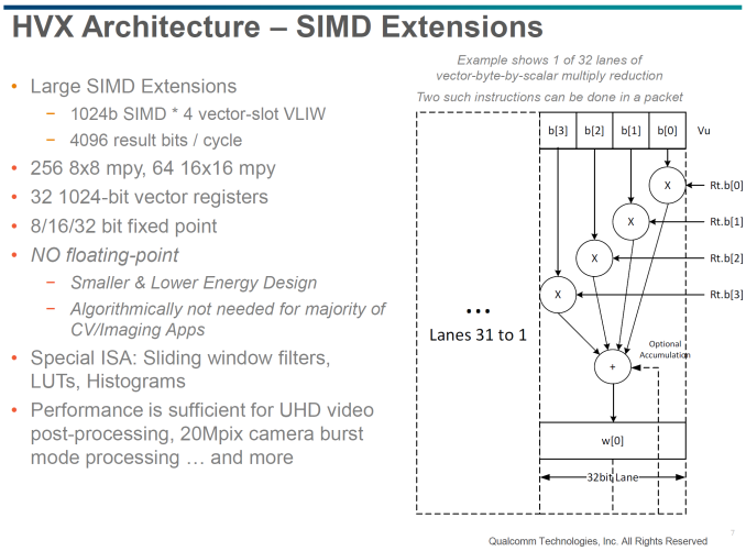
The HVX extension to Hexagon has 1024-bit vector data registers, with the ability to address up to four of these slots per instruction, which allows for up to 4096 bits per cycle. It's important to keep in mind that the instruction width is much smaller than this as this is a single instruction, multiple data (SIMD) unit which uses one operation over multiple chunks of data. There are 32 of these vector registers, which appear to be split between two HVX contexts. There is support for up to 32 bit fixed point decimal operations, but floating point is not supported to reduce die size and power consumption, as the previously mentioned applications for Hexagon 680 don’t need floating point support. As DSPs tend to have ISAs tailored for the application, the Hexagon 680 HVX units support sliding window filters, LUTs, and histogram acceleration at the ISA level. The performance of these units are said to be sufficient for 4K video post-processing, 20MP camera burst processing, and other applications with similar compute requirements.
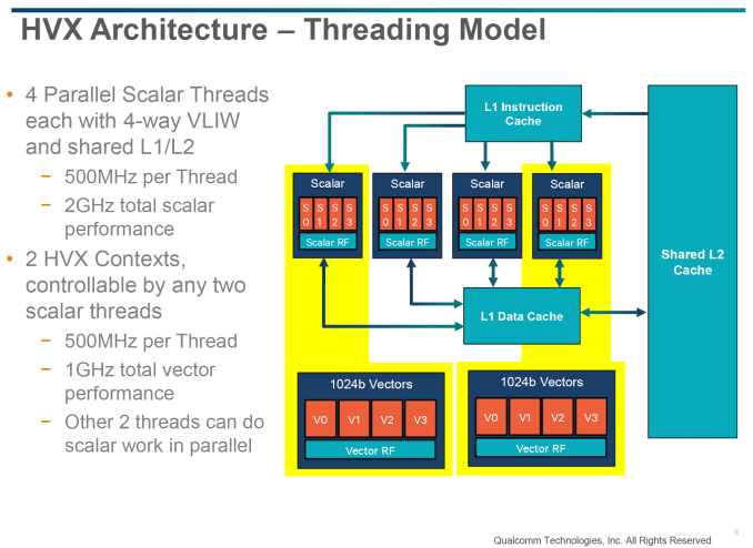
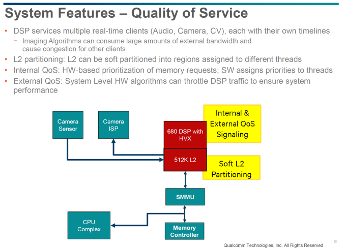
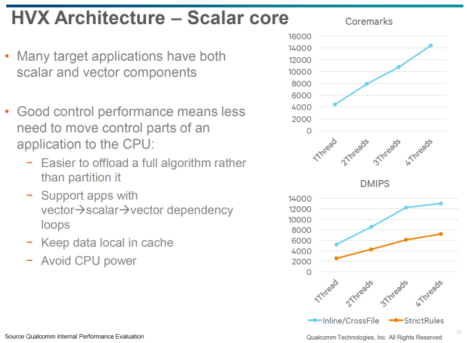
Outside of these details at a per-context basis, the threading model and memory hierarchy of the Hexagon 680 is quite unique. For scalar instructions, four threads are available with a 4-way VLIW architecture running at 500 MHz per thread. These scalar units all share an L1 instruction cache, L1 data cache, and L2 cache. The two HVX contexts in the Hexagon 680 can be controlled by any two scalar threads and also run at 500 MHz without stalling other scalar units not involved in controlling the vector units. This level of hardware-level multithreading along with QoS systems and L2 soft partitioning on a per-thread helps to make sure audio and imaging tasks aren’t fighting for execution time on the Hexagon DSP.
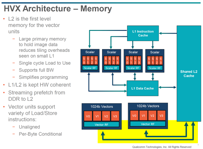
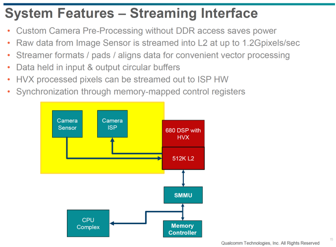
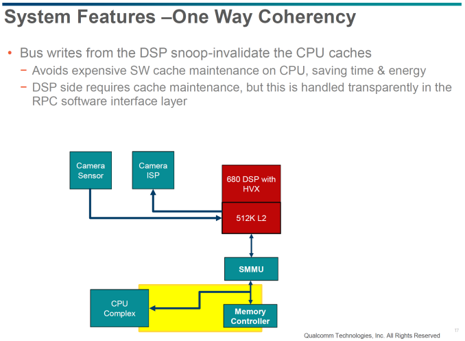
Meanwhile the vector units are fed exclusively from the L2 cache that is shared with the scalar units, a choice Qualcomm made due to the overhead that comes with an L1 cache for image processing workloads. This L2 cache can do load to use in a single cycle though, so one could argue that this is technically an L1 cache at times anyhow. The Hexagon 680 in the Snapdragon 820 will also be able to have data from the camera sensor directly streamed to the L2 cache and shared with the ISP to avoid the power cost of going off-die to DRAM. There’s also an SMMU (System Memory Management Unit) which allows for no-copy data sharing with the CPU for multiple simultaneous applications. DSP memory writes will also snoop-invalidate CPU cache without the need for the CPU to do any work involving cache maintenance to reduce power consumption and improve performance.
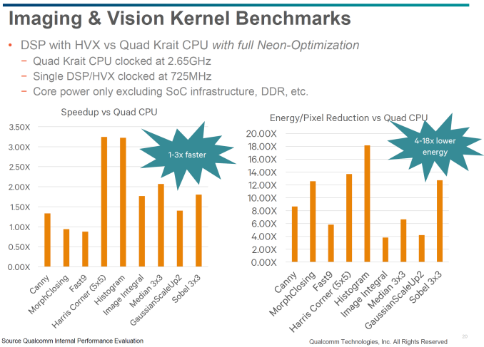
Relative to a quad-core Krait, the advantages of running some workloads on a DSP is enormous based on Qualcomm's internal benchmarks. According to Qualcomm, the NEON units in the Krait CPU are generally representative of NEON units within the industry, which is the reason why they've been used as the reference point here. Within a single logical “core”, Krait will only support 128-bit NEON with a single SIMD pipeline, compared to the 4-way, 1024-bit SIMD units of the Hexagon 680. SIMD threads also run on a 512KB L2-but-almost-L1 cache, as opposed to the 32KB L1 instruction/data cache of Krait, which helps to hide latency effects of DRAM. The NEON units of a Krait and many other ARM CPUs are capable of floating point, but in a workload like low light video enhancement Hexagon 680 will be able to complete the same amount of work at three times the speed, while using an order of magnitude less power due to the inherent advantages of a task-specific DSP architecture. The four scalar threads available in the DSP also means that entire algorithms can be off-loaded to the DSP instead of partially running on the CPU, which also reduces power consumption and makes it easier for developers to take advantage of the DSP.
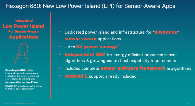
While Hexagon 680’s vector and scalar engines are useful for heavy-duty signal processing workloads, the addition of the low power island (LPI) DSP makes it possible to do away with separate sensor hubs in smartphones. According to Qualcomm, this DSP is completely separate from the scalar and vector compute DSP previously discussed (yet still part of the overall Hexagon DSP design), and sits on its own power island so the rest of the SoC can be shut down while keeping the LPI on. This also shouldn’t have a different process technology or a radically different standard cell library, as the advantages from the leading edge FinFET process should help significantly with power consumption.
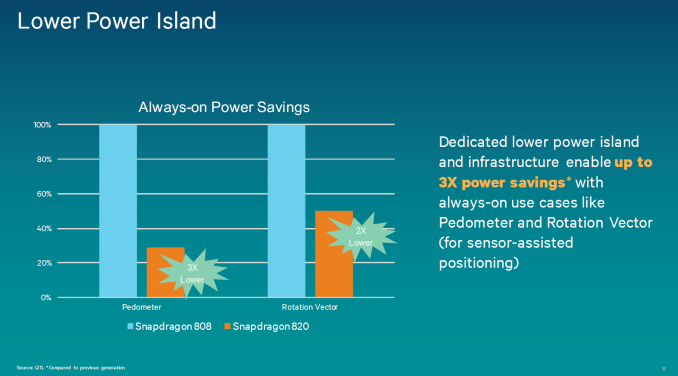
It’s said that this low power island with an independent DSP and newer process node is enough to improve power efficiency by up to three times in certain workloads compared to Snapdragon 808. I suspect that this was done instead of a comparison to the MSM8974/Snapdragon 800 generation because the Hexagon DSP was updated in the move from Snapdragon 805 to 808. Qualcomm emphasized the choice of a DSP over an MCU for this task, as in their internal testing a DSP delivers better power efficiency than a Cortex M-class MCU for more advanced sensor algorithms. The software stack for all of these features is already said to be quite complete, with a framework and algorithms included for OEM development. The broader Hexagon 600 series SDK is also quite extensive, with a number of utilities to allow for faster and easier development.
If you’re like me, after going through all of this information you might be wondering what the value of these vector DSP extensions are. In discussions with Qualcomm, it seems that the reasoning behind pushing a number of image processing tasks to the Hexagon DSP core is mostly because the algorithms behind things such as HDR video, HDR image merging, low light image enhancement, and other advanced algorithms are still in flux even from software update to software update. As a result, it isn’t viable to make these aspects of the imaging pipeline done in fixed-function hardware. Without the use of the Hexagon DSP, these tasks could potentially end up running on the CPU or GPU, affecting user experience in the form of higher shot to shot latency, reduced battery life when using the camera, and higher skin temperatures. It remains to be seen whether OEMs using Snapdragon 820 will use these DSPs to the fullest extent, but the Snapdragon 820 is shaping up to be a promising 2016 high-end SoC.
Read More ...
ECS LIVA x2 Review: A Compact & Fanless Braswell PC
The popularity of the NUC form factor has led to a resurgence in the nettop category. Thankfully, the core computing performance of the new systems have been miles ahead of the nettops of the past, and this has created an overall positive sentiment for the ultra-compact form factor (UCFF) in the minds of the consumers. ECS has been attempting to differentiate in the UCFF space with fanless systems using Mini Lake boards and custom-designed chassis in their LIVA series. The feature set and pricing of the LIVA units make it target the developing and cost-sensitive markets. We have already reviewed two of their Bay Trail-based systems, the original LIVA and the LIVA X. Read on to find out what ECS manages to deliver with the Braswell-based LIVA x2.
Read More ...
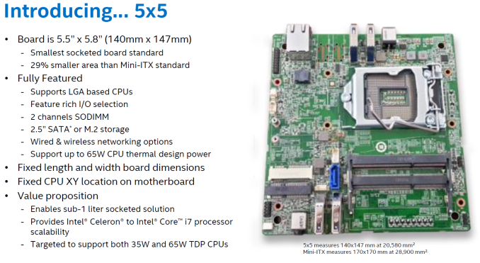
Intel Launches New Socketed 5x5 mini-PC Motherboards
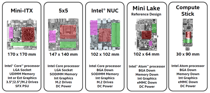
Over the last couple of years, the ultra-compact form factor (UCFF) has emerged as one of the bright spots in the troubled PC market. Kickstarted by Intel's NUC (Next Unit of Computing) designs, it has been successfully cloned by other vendors such as GIGABYTE (BRIX), Zotac (C-series nano) and ASRock (Beebox). With platform performance increasing every generation, and performance requirements getting tempered by the rise of the not-so-powerful smartphones and tablets, Intel could pack a heavy punch with their 102x102mm NUC motherboards.
Atom-based units (using Bay Trail) could provide very good performance for most users. Intel tried to shrink the PC even further by releasing a Compute Stick based on the Bay Trail Atom Z series SoCs earlier this year. ECS, with their LIVA designs, has adopted the Mini Lake reference design for their UCFF PCs. All of these UCFF PCs come with BGA CPUs / SoCs. The configurability aspect is minimal from an end-user's perspective. Looking at the mini-ITX form factor immediately leads us to a hole in the mini-PC lineup between it and the NUC.
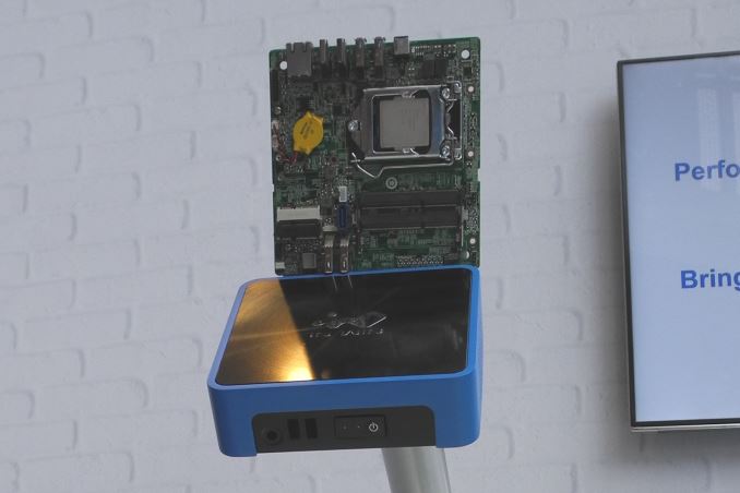
At IDF last week, Intel quietly launched the new 5x5 motherboard form factor. Coming in at 147x140mm, it is closer to the NUC in the fact that it can operate directly off DC power and takes SODIMM memory. Approaching from the mini-ITX side gives us the LGA socket for a Core processor. Unfortunately, at this size, we have to make do without the full length PCIe slot.
Intel suggests that solutions using the 5x5 boards could come in with a 39mm height for a volume of 0.89L (when using M.2 drives and a heat sink suitable for 35W TDP CPUs). 65W TDP CPUs and 2.5" drive support would obviously increase the height requirements.
Many usage areas which required custom-sized embedded boards (such as digital signage / point of sale terminals / kiosks etc.) have now opened up for the PC, thanks to the NUC and other similar form factors that were introduced over the last year or so. The new 5x5 form factor ensures that a mini-PC is available for every size and performance requirement. As of now, it looks like In-Win has a chassis design ready for the new form factor. We are awaiting more information on the board(s) and availability details.
Read More ...
Microsoft's Windows 10 Leaves Lumia 530 Behind w/ 8 GB Storage Requirement
Fate of Lumia '20 Series is Unclear
Read More ...
Future of Lumia Uncertain as Microsoft Lays Off 2,300, Closes 1 of 3 Finnish Offices
Product development will continue, but staff is substantially diminished from the levels it was at prior to the Nokia acquisition
Read More ...
Aluminum 7003, Used in Roofing, May be Tapped by Apple for iPhone 6S/6S+
New aluminum alloy is nearly three times as strong as the cheaper 6000 Series; Pink variant is rumored
Read More ...
Available Tags:Intel , Windows , Windows , Microsoft , Android , Motherboards , iPhone 6 , Apple , iPhone ,



No comments:
Post a Comment