
Nixeus NX-VUE24A 144Hz FreeSync Monitor Set to Ship
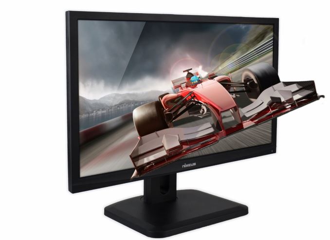
As a recap, the Nixeus NX-VUE24A is a 24" 1080p AMD FreeSync certified monitors with a minimum supported refresh rate of 30 Hz. The features of the NX-VUE24A include:
- 24" 1920 x 1080 TN panel
- Adaptive sync with refresh rates between 30 - 144 Hz
- 1ms response time
- DP 1.2a, HDMI, DL-DVI and VGA inputs
- Articulating stand for height adjustment (with tilt, pivot and swivel capabilities)
- 3-year warranty
AMD-certified FreeSync monitors come with a wide range of specifications and prices. Wikipedia has a list. Selected FreeSync models of relevance here (24" and 1080p resolution) include:
- The 24" 1920 x 1080 AOC G2460PF with a supposed refresh rate range of 30-160 Hz (availability outside Europe and pricing details are not known yet, and it appears that the maximum static refresh rate is only 144 Hz)
- The 24" 1920 x 1080 Samsung S24E370DL with a maximum refresh rate of 60 Hz (not yet available for sale in US, but a eBay listing puts a $400 price tag on it)
It appears that the Nixeus NX-VUE24A is the only 1920 x 1080 monitor currently available for purchase that comes with 30-144 Hz refresh rate support.
With a MSRP of $350 (and street price of around $330), the monitor seems to be priced right compared to other FreeSync monitors with similar feature sets. Pre-orders are being accepted at a number of e-tailers including Newegg, Amazon, and CouchPotato. CouchPotato seems to be offering free shipping and a new customer discount of 10%, while Newegg is charging $5 for shippping. Amazon seems to be selling at MSRP right now with free shipping.
Read More ...
HGST And Mellanox Show Off SAN Fabric Backed By Phase Change Memory

Last year at FMS, HGST showed a PCIe card with 2GB of Micron's Phase Change Memory (PCM). That drive used a custom protocol to achieve lower latency than possible with NVMe: it could complete a 512-byte read in about 1-1.5µs, and delivered about 3M IOPS for queued reads. HGST hasn't said how the PCM device in this year's demo differs, if at all. Instead, they're exploring what kind of performance is possible when accessing the storage remotely. Their demo has latency of less than 2µs for 512-byte reads and throughput of 3.5GB/s using Remote Direct Memory Access (RDMA) over Mellanox InfiniBand equipment. By comparison, NAND flash reads take tens of microseconds without counting any protocol overhead.

This presentation from February 2014 provides a great summary of where HGST is going with this work. It's been hard to tell which non-volatile memory technology is going to replace NAND flash. Just a few weeks ago Intel and Micron announced their 3D XPoint memory, immediately taking the place as one of the most viable alternatives to NAND flash without even officially saying what kind of memory cell it uses. Rather than place a bet on which new memory technology would pan out, HGST is trying to ensure that they're ready to exploit the winner's advantages over NAND flash.
None of the major contenders are suitable for directly replacing DRAM, either due to to limited endurance (even if it is much higher than flash), poor write performance, or vastly insufficient capacity. At the same time, ST-MRAM, CBRAM, PCM, and others are all much faster than NAND flash and none of the current interfaces other than a DRAM interface can keep pace. HGST chose to develop a custom protocol over standard PCIe as more practical than trying to make a PCM SSD that works as a DIMM connected to existing memory controllers.
Last year's demo showed that they were ready to deliver better-than-flash performance as soon as the new memory technology becomes economical. This year's demo shows that they can retain most of that performance while putting their custom technology behind an industry-standard RDMA interface to create an immediately deployable solution, and in principle it can all work just as well for 3D XPoint memory as for Phase Change Memory.
Read More ...
NVIDIA Releases 355.60 Drivers; GameWorks VR Now In Beta
This latest release is notable for a few different reasons. Officially NVIDIA is releasing this as their preferred Game Ready driver for the Ashes of the Singularity tech demo, which is due later this month. Ashes is a large-scale RTS being developed by Oxide Games and Stardock, the former of which is likely better known for their Star Swarm tech demo. Built on the same Nitrous engine, Ashes will be the first DirectX 12 enabled consumer software to be released, though in very early form as a tech demo ahead of its 2016 launch.

Meanwhile this driver is also the first release from NVIDIA’s R355 branch. At this point we don’t know a great deal about this new driver branch – NVIDIA’s release notes are thin on both new features and bug fixes – though I suspect this is one of those cases where we’ll find out more later.
That said, the one major addition we do know about for this driver is that it enables support for NVIDIA’s GameWorks VR technology in a consumer driver. Along with this driver release GameWorks VR is being promoted from alpha to beta status, and with the release of a new beta SDK is being opened up to more developers and wider testing. NVIDIA has been heavily investing in VR, seeing it as a potential new market to not only further grow sales, but as a market that will require more powerful and expensive GPUs than standard consumer system builds.
As usual, you can grab the drivers for all current desktop and mobile NVIDIA GPUs over at NVIDIA’s driver download page.
Read More ...
Hands On With the Samsung Galaxy Note 5 and Samsung Galaxy S6 edge+
Today, Samsung is announcing the next generation of their Galaxy-brand phablets, the Galaxy Note 5 and the Galaxy S6 edge+. Samsung’s phablets have been one of their greatest smartphone success stories, finding traction in a market when many thought there wouldn’t be a place for such a large phone. And while you will never see some competitors directly admit to it, products like the Note series have legitimized the phablet form factor and required that the competition catch up as well, making the phablet form factor as much of a home court for Samsung as there can be.
Starting with the 2014 models, Samsung introduced two different phablets, the Note 4 and the simply titled Note Edge. This year Samsung is retaining the dual phablet approach, however in the case of the Edge product Samsung has shifted gears on what they want to do. For 2015 Samsung seems to be going after a new audience in the form of the Galaxy S6 edge+, which is a more distinct derivative of the Note 5 platform with some greater feature changes than just a curved screen. To understand what I mean, read on for the full article.
Read More ...
Samsung SSD Update: 48-layer 256Gbit TLC 3D NAND & Three New TLC SSDs Announced
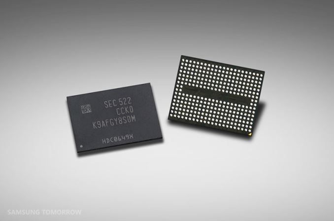
We knew that Samsung's third generation of V-NAND/3D NAND was on the way with mass production scheduled for the second half of this year. Samsung has now disclosed that mass production is starting this month, and that it's a 48-layer design with a 256Gb TLC being the first die announced. Samsung's current second-generation 3D NAND is a 32-layer design available as 128Gb TLC or 128Gb MLC.
With mass production imminent, Samsung has ensured that neither SK Hynix nor the Toshiba/SanDisk joint venture will be able to leapfrog them with their respective 48-layer 3D NAND designs, both scheduled for mass production starting in 2016.
Samsung says the new 256Gb TLC will have about 30% lower power consumption than an equivalent capacity of their current 128Gb TLC, and a switch to a dual-plane organization ensures that one 256Gb die will perform at least as well as a pair of the current 128Gb dies. Density is improved by about 40% while production costs only increased slightly, so price per GB will be going down. At FMS, Samsung is pushing the idea that their 3D NAND TLC is ready to replace MLC for most uses, and they're optimistic about scaling up their 3D NAND layer count past 100.
| New Samsung 48-Layer TLC SSDs | |||
| Drive | PM953 | PM1633 | PM1725 |
| Form Factor | NVMe over M.2 22110 and 2.5" | 2.5" SAS 12Gb/s | NVMe PCIe HHHL card |
| Capacities | 480GB, 960GB, 1.92TB (2.5" only) | 480GB, 960GB, 1.92TB, 3.84TB | 3.2TB, 6.4TB |
| Sequential Read | ? | 1,100 MB/s | 5,500 MB/s |
| Sequential Write | ? | 1,000 MB/s | 1,800 MB/s |
| 4kB Random Read IOPS | ? | 160k | 1,000k |
| 4kB Random Write IOPS | ? | 18k | 120k |
| Endurance Rating | ? | ? | 5 DWPD (6.4 TB model) |
Samsung also shared information about three upcoming drives, all using TLC though not necessarily the new 48-layer parts. The PM1633 Enterprise SAS drive was previewed at CES in January and is intended for read-heavy workloads. A follow-on PM1633a model was mentioned to use the new 48-layer TLC to reach 15.36TB capacity, but we don't have any other information about that update. The PM953 is a enterprise NVMe drive in M.2 or 2.5" form factors, and is the counterpart to the MLC-based SM951. Of particular interest, the M.2 version is using the M.2 22110 form factor (22mm x 110mm, the maximum length for M.2), with Samsung using the extra space to implement power loss protection.
Meanwhile the PM1725 is a fast multi-TB PCIe expansion card that Samsung intends to use to challenge the assumptions about what uses TLC is suited for. Relatively speaking it appears to be intended for workloads that aren't very write-heavy, but it still manages 120k IOPS for writes. That just looks small compared to 1M IOPS for reads and a sequential read speed of 5.5GB/s.
All three drives are intended for OEMs, but the PM953 will probably find its way into the retail channel just like the SM951.
Finally, along with Samsung's new 3D NAND appearing in the afformentioned new drives, it will also be appearing in at least one of their existing drives. The 850 EVO, Samsung's current consumer TLC drive, will apparently be getting an update to use the new 48-layer TLC, though it's not clear if this will be new capacities and/or a wholesale NAND update.
Read More ...
Qualcomm Details the Adreno 530 GPU and ISP inside the Snapdragon 820
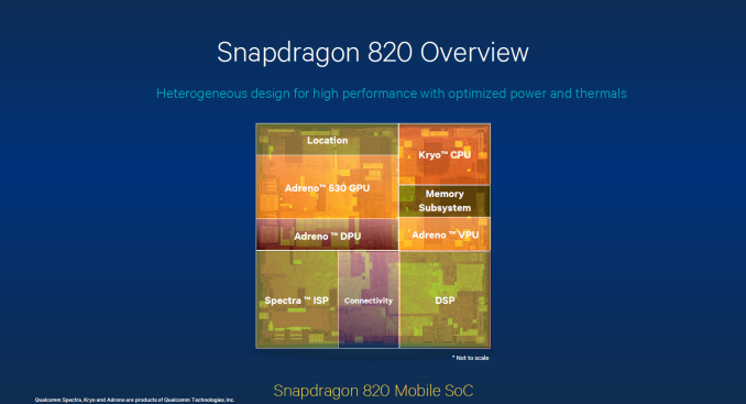

Because Adreno 530 is their new flagship GPU, Qualcomm's press release focuses more on the 530 than the 510. The performance figures released by Qualcomm describe Adreno 530 as being 40% faster than Adreno 430 on average, while also consuming 40% less power. This result is described as an average of "the top graphics benchmarks", and while it's still generally a good idea to take vendor provided numbers with a grain of salt, if the power and performance gains over Adreno 430 are anywhere in the ballpark of Qualcomm's 40% figure then Adreno 530 should end up being quite impressive.

On the API side, Adreno 500 series GPUs will support OpenGL ES 3.1 + AEP (Android Extension Pack), Renderscript, Vulkan, and OpenCL 2.0. With OpenCL 2.0 comes support for Shared Virtual Memory (SVP), which allows an OpenCL host program and a device's kernel to share a virtual address space so access to data structures like lists and trees can be easily shared between the host and GPU. Adreno 530 has varying improvements to GPGPU performance when compared to Adreno 430, but Qualcomm's slides show video processing as demonstrating the greatest improvement with a 2.5x increase in compute performance. This is also the area where efficiency gains for generational improvements typically happen, so we expect fixed-function codec support although this information is not yet provided.
As for the ISP, it's still the case that mobile image signal processors are black boxes. Qualcomm is stating that their Spectra ISP in Snapdragon 820 will be able to support 3 simultaneous cameras at up to 25MP and at 30fps with no shutter lag. The Spectra ISP will also use MIPI's higher bandwidth C-PHY serial interface, which supports the enhanced camera support. As well as this, new developer and user-facing features include support and APIs for depth maps and using dual cameras to perform refocusing or other visual effects - because Qualcomm is just the SoC manufacturer, it is up to the smartphone OEMs to implement dual-camera/depth-maps as a feature as well.
According to Qualcomm, Snapdragon 820 will start showing up in devices during the first half of 2016. Hopefully between now and then there's more information from Qualcomm about the other aspects of their new SoC, including their Kryo custom CPU core. In Q1 we will be at Mobile World Congress, so we may see more information at that time.
Source: Qualcomm, slides via Slashgear
Read More ...
Toshiba Brings Through-Silicon Vias to NAND Flash
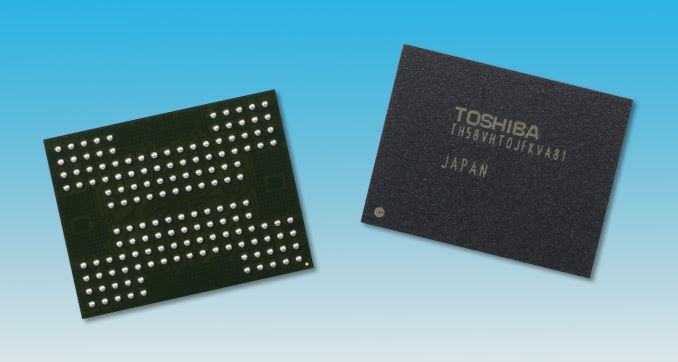
The NAND flash currently on the market is typically produced in the form of a die with a capacity like 128Gb (16GB). The popular SSD form factors don't have enough surface area to fit dozens of those chips, and SSD controllers don't have the pin count to connect to that many independently, so several chips are stacked in a single postage-stamp sized package. The traditional way of connecting the individual dies in a stack is to use the same technique as for a single-die package: bonding a thin gold wire between the edge of the die and the package substrate or external pins. The downsides are that it requires a lot of wires and the edges of the dies in the stack need to be exposed somehow, either by staggering them or by putting a spacer between each layer.

An alternative packaging method is to design the dies to participate in the stacking, by including electrical conductors that penetrate the entire thickness of the silicon die so that they can make contact with the dies above and below it in the stack, essentially tunneling right through each die. These through-silicon vias (TSVs) can then form a shared bus to carry signals from any of the dies in the stack out to the last die, which is the only one with the external connections.

Chip stacking using TSVs requires the dies to be aligned and stacked without spacers, which makes the whole stack a bit more compact. Since TSVs can be placed anywhere on the chip rather than just at the edge, it's easy to implement a wide data bus and communication within the stack can be very fast or low-power due to the short distances involved. These advantages have been very attractive for packaging DRAM, most notably in the form of the HBM stacks used by AMD's R9 Fury and R9 Nano video cards.
Toshiba's demonstration is a 16-high stack of 128Gb dies in a BGA-152 package measuring 14mm by 18mm and 1.9mm thick, and an 8-high stack that's 1.35mm thick. Those numbers are all typical even for wire-bonded stacks. The speed (1Gb/s) and operating voltages (1.2V for I/O and 1.8V core) are what we would expect from a next-generation NAND interface, but the claimed 50% power reduction is a very nice improvement for a change that leaves the flash memory cells themselves unmodified.
Toshiba hasn't said whether the dies being stacked are their current 15nm planar NAND or their forthcoming 3D NAND, nor have they said when modules using TSVs will be hitting the market. The most compelling applications would be to use TSVs to stack flash atop a controller chip in an eMMC product or atop an SoC, but the power savings would be appreciated almost everywhere. If the use of TSVs allows economically stacking more than 16 dies, it could enable a dramatic increase in the density of SSDs.
Read More ...
Advatronix Nimbus 400 File Server Review
Small businesses and power users often need the flexibility offered by a file server when compared to a dedicated NAS. This is where storage servers based on Microsoft's Windows Server offerings and systems based on various Linux and BSD distributions come into play. These servers can be bought as an appliance or assembled in a do-it-yourself (DIY) fashion. Today, we will be looking at a system based on the former approach - the Advatronix Nimbus 400.
Read More ...
Build-A-Rig Round 1: The Winners

- Zotac’s Hey Good Lookin’: Adam Abadir of Austin, TX
- Corsair’s The Accelerator: David Baron of Gilbert, AZ.

Congratulations to our two winners, and the first winners for the Build-A-Rig project. And be sure to check back later this month when we kick off Build-A-Rig round 2, where we will be putting together and giving away a pair of small form factor systems.
Read More ...
Kentucky Man Faces up to 10 Years in Prison for Shooting Drone Trespasser
Drone was hovering over his property, appeared to be filming defendant's daughters; owner confronted him but was not charged
Read More ...
Windows 10 on Raspberry Pi, IoT Devices Sees Developer Debut
"It's Windows, Jim, but not as we know it!"
Read More ...
Available Tags:NVIDIA , Samsung , Galaxy , Samsung , Galaxy , SSD , 3D , GPU , Toshiba , Server , Windows ,
No comments:
Post a Comment