
AMD Announces OEM Desktop Radeon 300 Series
We’ve been through this event once before – most recently with the OEM HD 8000 series – so our regular readers will know the drill. Whether or not GPU manufacturers have new GPUs, OEMs will want new parts to sell, which leads to GPU manufacturers engaging in rebranding and subtle spec changes to create new parts to sell under a new series name. In AMD’s case this is complicated by the fact that they have been updating their GPUs in a piecemeal fashion – Hawaii, Bonaire, and Tonga have all landed at very different times – and AMD is not done yet as they’re going to be launching a new high-end GPU this quarter. So AMD needs a product lineup to include both the new part and their retained parts under a single brand, which leads to another incentive for rebadging.
In any case, as these are OEM parts I advise not reading into the names and specifications too much. AMD’s OEM and Retail parts can be very different at times – and at other times there aren’t any retail parts at all (HD 8000) – so these OEM parts aren’t necessarily indicative of what we’re going to see in retail in the coming months. Though based on AMD’s actions with the Radeon 200 series, we may yet see a similar rebadge happen for the retail 300 series.
| AMD OEM Desktop Radeon R9 300 Series | |||||
| AMD Radeon HD R9 380 OEM | AMD Radeon R9 370 OEM | AMD Radeon R9 360 OEM | |||
| Was | Variant of R9 285 | Variant of R7 265 | Variant of R9 260 (OEM) | ||
| Stream Processors | 1792 | 1024 | 768 | ||
| Texture Units | 112 | 64 | 48 | ||
| ROPs | 32 | 32 | 16 | ||
| Boost Clock | <=918MHz | <=975MHz | <=1050MHz | ||
| Memory Clock | 5.5GHz GDDR5 | 5.6GHz GDDR5 | 6.5GHz GDDR5? | ||
| Memory Bus Width | 256-bit | 256-bit | 128-bit | ||
| VRAM | <=4GB | 2GB/4GB | 2GB | ||
| Transistor Count | 5.0B | 2.8B | 2.08B | ||
| GPU | Tonga | Pitcairn | Bonaire | ||
| Manufacturing Process | TSMC 28nm | TSMC 28nm | TSMC 28nm | ||
| Architecture | GCN 1.2 | GCN 1.0 | GCN 1.1 | ||
Starting things off, we have the OEM R9 series. Today’s release tops out at R9 380 OEM (I can only imagine AMD is saving 390 for their new GPU), along with the R9 370 OEM and R9 360 OEM. The R9 380 OEM appears to be a variant of the desktop R9 285, which marks the first time that a Tonga card has been released in an OEM configuration. The quoted clockspeeds are identical to the retail R9 285, which means the “up to” GPU clockspeed should result in the R9 380 OEM being perfectly identical to the R9 285 if given its maximum configuration.
Meanwhile for the R9 370 OEM we have a cut-down Pitcairn card, with only 1024 of its 1280 SPs active. This makes it a variant of the retail R7 265, though with a slightly higher maximum GPU clockspeed. Truth be told I’m a bit worried to see a fresh Pitcairn part in 2015; Pitcairn has been a workhorse for AMD, having now survived into its 4th generation of cards. However at over 3 years old and based on GCN 1.0, it lacks more modern functionality such as the ability to decode 4K H.264 video files, AMD’s improved power management technology, and support for AMD’s Freesync technology.
Finally we have the R9 360 OEM. This appears to be a variant of the R9 260 OEM, featuring an AMD Bonaire GPU with only 768 of its 896 SPs enabled. Oddly, the listed memory bandwidth for the part, 104GB/sec, would require 6.5GHz GDDR5 memory given Bonaire’s 128-bit bus. I suspect that may be an error on AMD’s part, though it’s not outside the realm of possibility. In any case the R9 360 OEM also appears to be a regression from the R9 260 OEM; the latter was a fully enabled Bonaire part, whereas this one is not. At the very least it’s GCN 1.1 based, so it will have the newer features that the Pitcairn based R9 370 OEM lacks.
| AMD OEM Desktop Radeon R7 300 Series | ||||
| AMD Radeon HD R7 350 OEM | AMD Radeon R7 340 OEM | |||
| Was | R7 250 | R7 240 | ||
| Stream Processors | 384 | 384 | ||
| Texture Units | 24 | 24 | ||
| ROPs | 8 | 8 | ||
| Boost Clock | <=1050MHz | <=780Hz | ||
| Memory Clock | <=4.5GHz GDDR5 ?GHz DDR3 |
<=4.5GHz GDDR5 ?GHz DDR3 |
||
| Memory Bus Width | 128-bit | 128-bit | ||
| VRAM | 1GB/2GB | 1GB/2GB GDDR5 2GB/4GB DDR3 |
||
| GPU | Oland | Oland | ||
| Manufacturing Process | TSMC 28nm | TSMC 28nm | ||
| Architecture | GCN 1.0 | GCN 1.0 | ||
Up next is the R7 300 OEM series, which is composed of the R7 350 OEM and R7 340 OEM. Both of these cards are straight-up rebadges of AMD’s existing R7 250 OEM and R7 240 OEM parts, and both are based on the same GCN 1.0 Oland GPU. With just 384 SPs these are low cost, low performing parts. The difference between the two is their clockspeeds, with R7 350 being clocked quite a bit higher, whereas R7 340 is clocked lower in exchange for being available as a low-profile card. Unfortunately the memory situation is quite complex here, as these cards can be equipped with either GDDR5 or DDR3; the GDDR5 versions will of course be the much faster versions.
Among its other quirks, Oland lacks a hardware video decoder. So these parts are likely to be paired with low-end AMD Kaveri APUs, possibly for a Dual Graphics configuration.
| AMD OEM Desktop Radeon R5 300 Series | ||||
| AMD Radeon HD R5 340 OEM | AMD Radeon R5 330 OEM | |||
| Was | Variant of R5 240 | Variant of R5 240 | ||
| Stream Processors | 320 | 320 | ||
| Texture Units | 20 | 20 | ||
| ROPs | 8 | 8 | ||
| Boost Clock | <=825MHz | <=855Hz | ||
| Memory Clock | ? GDDR5/DDR3 | ? DDR3 | ||
| Memory Bus Width | ? | ? | ||
| VRAM | <=2GB GDDR5/DDR3 | <=2GB DDR3 | ||
| GPU | Oland | Oland | ||
| Manufacturing Process | TSMC 28nm | TSMC 28nm | ||
| Architecture | GCN 1.0 | GCN 1.0 | ||
Finally, for the R5 300 OEM series we have two more Oland parts. These are ultra low end, low-profile single slot parts. AMD does not even publish the GPU bandwidth numbers for these parts, and as a result I suspect these may be 64-bit parts to further cut down on costs. Of particular note, the R5 330 lacks HDMI support, so it’s almost certainly geared towards APAC markets where VGA is still in common use.
Wrapping things up, AMD's press release mentions that these new OEM parts are shipping now. HP is already confirmed to be shipping PCs with these new cards, and we expect other OEMs to ramp up as well as they launch their back-to-school season computers.
Read More ...
Update: AMD Announces Radeon M300 Series Notebook Video Cards
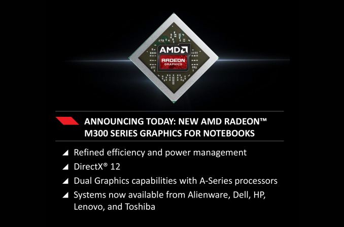
Being announced today is the Radeon M300 series. With so much other news coming out of FAD we’re still tracking down more information on the product line, but of the information released by AMD so far, we do know that these parts are being advertised as refined parts with better efficiency and power management. AMD’s FAD presentation has not made any mention of what specific GPUs are being used here or of specific SKUs (we may yet see a press release), so it’s not clear whether there are new GPUs involved or if these are simply rebadges of existing GPUs and products.
AMD does note that M300 systems should already be available from several of AMD’s usual partners, including Alienware, HP, Dell, Lenovo, and Toshiba. Meanwhile given the timing of the announcement and the fact that AMD is specifically advertising these GPUs as supporting Dual Graphics mode with AMD’s A-series APUs, I suspect some of these GPUs may be intended to work alongside AMD’s Carrizo APU, which is due this year.
Update: AMD has since released the details of the M300 SKUs on their website, and though they’re not incredibly detailed, they give us an idea of just what AMD is up to.
| AMD M300 Series GPU Specification Comparison | |||||
| R9 M375 | R7 M360 | R5 M330 | |||
| Was | Variant of R9 M270/M260 | Variant of R7 M270/M260 | Variant of R5 M255 | ||
| Stream Processors | 640 | 384 | 320 | ||
| Texture Units | 40 | 24 | 20 | ||
| ROPs | 16 | 4? | 4? | ||
| Boost Clock | <=1015MHz | <=1015MHz | <=1030MHz | ||
| Memory Clock | 2.2GHz DDR3 | 2GHz DDR3 | 2GHz DDR3 | ||
| Memory Bus Width | 128-bit | 64-bit | 64-bit | ||
| VRAM | <=4GB | <=4GB | <=4GB | ||
| GPU | Cape Verde | Oland | Oland | ||
| Manufacturing Process | TSMC 28nm | TSMC 28nm | TSMC 28nm | ||
| Architecture | GCN 1.0 | GCN 1.0 | GCN 1.0 | ||
Unfortunately it looks like everything is going to be a rebadge/rehash of AMD’s existing GCN 1.0 GPUs. While AMD’s specs do not confirm which GPUs we’re looking at, and hence we’re admittedly taking an educated guess, based on the specs and features we have every reason to believe we’re looking at Cape Verde and Oland, the two GPUs that also backed AMD’s M200 series. I had been hoping for a cut-down Bonaire in here, to bring GCN 1.1 to mobile, but it doesn’t look like that’s in the cards.
What we have then is a 3 product stack with some very unusual configurations. Compared to their M200 counterparts, all 3 M300 parts have much higher GPU clockspeeds. AMD is now allowing clockspeeds over 1GHz, even for the low-end M330. Though as always, we need to remind everyone that these are “up to” speeds, and OEMs get the final choice in what the shipping clockspeed of a M300 part will be in any given laptop.
And although clockspeeds are up, memory bandwidth is way, way down. All of these parts ship with DDR3, and of those only the M375 gets a 128-bit memory bus. The other two parts, based on Oland, are shipping with a 64-bit memory bus. On the M200 series AMD was using GDDR5 with Cape Verde and the full 128-bit memory bus with Oland, so these new parts have half (or less) of the memory bandwidth of their M200 counterparts. The fact that AMD did this while increasing clockspeeds (which generally has a knock-on impact on power consumption) is very odd, and I would expect that these new parts are going to be bandwidth starved and will not reach the full potential of their respective GPUs. Meanwhile there's also some uncertainty over the number of ROPs enabled on the M360 and M330; with 64-bit memory buses on a chip that natively has a 128-bit memory bus, AMD may have disabled half of the ROPs in the process.
Looking at these parts overall, in AMD’s FAD event today the company specifically noted the dual graphics capabilities of the M300 series, and I suspect that’s precisely what these parts are meant for. They’re not intended to be stand-alone, but rather they’re designed to be paired with Carrizo/Kaveri APUs to inject more graphics silicon to improve GPU performance. In which case we’re looking at another wrinkle in performance, not only from dual graphics but from the fact that AMD’s APUs tend to be hungry for bandwidth as well, in which case the impact of these slower memory buses may not be as great.
Finally, it’s interesting to note that AMD only went up to M375 here. They did not introduce an M380 or M390 series part, not even rebadging the Pitcairn/Tonga parts that compose the faster members of the M200 series. This may be a sign that AMD intends to introduce faster parts later on, but for the moment that’s merely speculation on my part.
Read More ...
AMD Financial Analyst Day 2015 Round-Up
Having just wrapped up a bit ago is AMD’s 2015 Financial Analyst Day (FAD). For AMD FADs are a combination of roadmap updates and number breakdowns for financial analysts and investors, showcasing where the company intends to go and why investors should continue to back the company.
We’ve been covering FAD 2015 throughout the afternoon, and we have seen AMD make a number of announcements and roadmap reveals throughout the event. The individual announcements are below, and meanwhile now that the event has wrapped up we want to provide a quick summary of what AMD is going to be up to over the next two years.
AMD Charts Future Growth Opportunities
AMD’s 2016-2017 x86 Roadmap: Zen Is In, Skybridge Is Out
AMD’s K12 ARM CPU Now In 2017
AMD’s 2016 GPU Roadmap: FinFET & High Bandwidth Memory
AMD To Launch New Desktop GPU This Quarter (Q2’15) With HBM
AMD Announces 6th Generation A-Series APU Branding - Carrizo Due This Quarter
AMD’s 2016-2017 Datacenter Roadmap: x86, ARM, and GPGPU
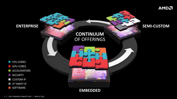
With AMD’s FAD 2012 being a major event for the company – one where then-CEO Rory Reed announced AMD’s intention to move away from being almost solely PC focused to a mix of PC, semi-custom, and ARM products – FAD 2015 by comparison is a far more tame event. Under the direction of Dr. Lisa Su, AMD is largely executing on the plan they set into motion some time ago. And where they have made changes, such as dropping SeaMicro, AMD has announced those changes in advance. So this year’s FAD does not see AMD announcing major changes to the company’s direction.

So what is AMD’s direction over the next two years? The short answer to that is that the company is focusing on what they believe to be higher margin, higher growth opportunity markets where they can take a chunk of those markets without necessarily having to wrest revenue and sales from existing competitors. Overall AMD sees their three big growth markets as gaming, immersive platforms, and the datacenter market.
At the same time what AMD is looking to avoid is low-margin markets where they can’t do something to set themselves apart. AMD has made it clear that they’re not going to invest in fields such as mobile (smartphones/tablets) or IoT client devices, as while that’s a high growth field, it’s already overweight with competitors who either have the cost control (MediaTek) or the war chest (Intel) to drive margins down to levels AMD cannot sustain. Similarly, AMD is working to reduce their presence in the low-end PC market, as that too suffers from low margins, and is coupled with a poor outlook that has seen AMD get burnt by a significant drop in demand (and consequently revenue) in that market.

The one exception to this of course is semi-custom silicon, which although is not high-margin, allows AMD to leverage their strengths. Nowhere else can you find a vendor with a top-tier GPU profile, custom x86 CPUs, custom ARM CPUs, and the willingness to help customers build customized chips around those building blocks. Semi-custom silicon also presents AMD with some relatively stable revenue, as contracts for semi-custom designs will typically involve supplying chips for a number of years.

To achieve their goals, AMD has set out a roadmap through 2016 and 2017 to develop the technologies necessary to compete in their respective markets, and to deliver the performance necessary for both semi-custom silicon and finished AMD products.

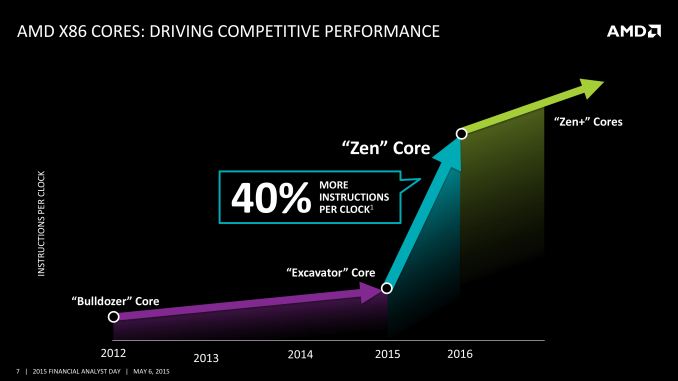
The big item on AMD’s agenda is of course Zen, the company’s forthcoming x86 CPU design. Scheduled to launch in 2016, starting with the high-performance desktop, Zen is a return to fundamentals of sorts for AMD. We do not have performance estimates for Zen, but from an architectural standpoint AMD is making it clear that they are shooting for much higher IPC with Zen than Carrizo/Excavator, touting a 40% increase in IPC.
Zen will ultimately be driving AMD’s entire range of x86 products, top to bottom, datacenter to laptop. AMD’s Dozer and Cat families are at an end, and in the end there will be only Zen. Zen in turn will be part of a long-term process for AMD; the company already has newer iterations of Zen in the works (Zen+) which further improve on the architecture farther out. Coupled with significant gains AMD is expecting to enjoy from FinFET processes, and the company is putting on their optimistic face for their chances in the x86 market.

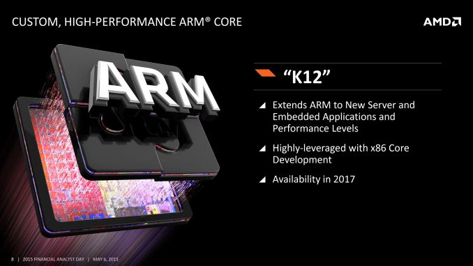
In fact AMD is backing Zen to the point where other projects have been pushed to the wayside or canceled altogether. AMD’s project Skybridge – a plan for 20nm ambidextrous x86 and ARM CPUs – has essentially been canceled as a result of the combination of lack of customer need for ambidextrous CPUs and the generally poor performance of the 20nm process. Meanwhile Zen’s ARM sibling – K12 – has been pushed back from 2016 to 2017 to allow AMD to complete Zen first, and then roll what they’ve learned from Zen into K12.
For AMD this marks a return to form, and a very aggressive move on the x86 market. After having seen their datacenter market share fall to just 1.5%, for example – with the company admitting they did not invest in high-performance CPUs and it cost them most of their market share – AMD is optimistic that they can recover their datacenter market share through the combination of Zen, K12, and their GPGPU capabilities. This in turn means hitting the datacenter in both the CPU and HPC markets, and even going one step beyond with a forthcoming, very high performance HPC APU that combines all of AMD’s strengths.

Meanwhile on the GPU front, AMD is not providing quite as much visibility on their GPU roadmap, but they are sharing their plans out to 2016. Launching this quarter will be a new AMD desktop product featuring High Bandwidth Memory (HBM), the first such product in the GPU space. HBM promises to significantly increase AMD’s available memory bandwidth and allow their partners to work on more innovative card designs due to the smaller amount of space an HBM solution requires.
2016 in turn will see AMD continue their focus on HBM with the release of products using HBM Gen2, all the while releasing their first GPUs manufactured on a FinFET process. AMD isn’t naming which process they’re using, though either way it would be a significant step up in manufacturing from the current 28nm process their GPUs use. Overall AMD is touting a 2x increase in perf-per-watt for their 2016 GPUs, with most of that gain coming from the shift to FinFET.
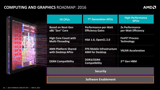
Longer term, while AMD is not committing towards any specific products, AMD is strongly hinting at HBM coming to APUs as well. AMD’s APUs have traditionally struggled under the limited amount of bandwidth 128-bit DDR3 provides, so an HBM-enabled APU would help to further improve AMD’s GPU performance on their APUs.
Wrapping things up, the key to AMD’s plans for the next two years will hinge on both properly anticipating the market and in executing on technology. AMD will need to correctly predict opportunities to grow – particularly rapidly expanding markets as opposed to stealing revenue from existing players – and then execute on that in a timely manner with solid hardware across both the CPU and GPU space. AMD believes they have the pieces they need in development, and with 2015 almost half-over the company is finally reaching the point where their earlier transition is complete, so it will be interesting to see how AMD’s next two years unfold. The company is not yet in dire straits, but after losing market share and seeing gross margins suffer, now is the time where AMD needs to reverse their fortunes and reach profitability if they’re to ensure their own future.


Read More ...
AMD’s 2016-2017 Datacenter Roadmap: x86, ARM, and GPGPU
Forrest’s comments on the embedded and semi-custom businesses generally reflected AMD’s earlier comments on their three growth opportunities, but I wanted to call specific attention to AMD’s datacenter plans, which Forrest we into in more detail.

AMD’s datacenter plans for the next couple of years will see AMD taking a three-pronged approach to the market. On the CPU side, AMD will of course be leveraging their forthcoming x86 Zen and ARM K12 CPU designs in various fashions. Zen, as previously discussed, should offer a significant increase in IPC and improve AMD’s competitive positioning in the x86 space. And since AMD is launching their high-performance desktop Zen CPU as the first Zen product, the implication is that the server version of that product should not be too far behind.

Meanwhile over the next couple of years AMD will be leveraging the Opteron A1100 “Seattle”, followed by the K12 in 2017. AMD is positioning their ARM datacenter products as being primed for efficiency, whereas their x86 products are primed for high native I/O capacity and high overall performance. Opteron A1100 will ship later this year, though I’m still unsure just how much adoption it is going to see as opposed to the K12 in 2017.

Last but certainly not least however, I wanted to call attention to AMD’s GPU/APU plans in the datacenter space. AMD already has a presence with GPU accelerator cards in the form of the FirePro S-series, with these cards being the basis of their high performance computing (HPC) and virtual desktop infrastructure (VDI) initiatives. AMD is expecting these markets to continue to grow as customers increasingly turn towards GPUs for better compute throughput, and VDI for remote client hosting and the server-side use cases it was designed for.
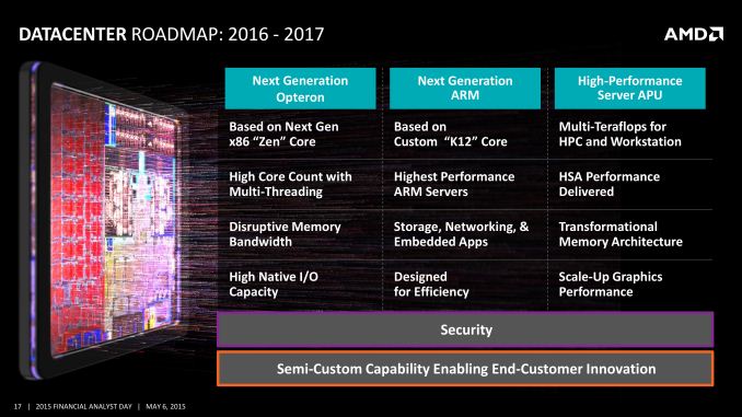
But the most interesting thing about this roadmap is AMD’s “high-performance server APU”. To date, the closest AMD has come to a server APU is are their FirePro APUs, which are versions of AMD’s standard desktop APUs with the ability to use their FirePro driver set and are intended for workstations. Consequently the creation of a high-performance server APU represents a new product within AMD’s portfolio, as they have never done something quite like this before.
AMD isn’t saying much about this APU, but it will be a multi-teraflops chip for both HPC and workstations, which implies something significantly more powerful than today’s Kaveri APUs, and much closer to the performance of some of AMD’s discrete GPUs. The end-game here of course is to leverage HSA and the close proximity of CPU and GPU in a way no other vendor currently can, to deliver high performance in workloads that benefit from close CPU/GPU interaction. The fact that AMD is targeting this at HPC makes me curious just what they’re planning for FP64 performance, but they could just as well be going after markets such as oil & gas and machine learning where FP32 and F16 are sufficient. Meanwhile there is also a very good reason to suspect that this may be the first place AMD implements HBM for an APU, as it would be in-line with their previous comments about doing HBM with more than just discrete GPUs, and this is a high-margin market that would be suitable for a higher-cost feature like HBM.

Ultimately for AMD their plans for the datacenter are ambitious, but if executed well seem to be achievable. After being pushed out of the x86 server market, AMD is making a concentrated effort to re-enter it via the Zen CPU, and AMD’s APUs offer an interesting, alternative take on getting there. That said, we should also expect to see AMD significantly leaning on open industry standards to get back into the datacenter space, and consequently making part of their argument the fact that they are not Intel, and consider themselves to be more open towards working with partners and customers.
Read More ...
Oculus Targets Q1 2016 for Consumer Oculus Rift
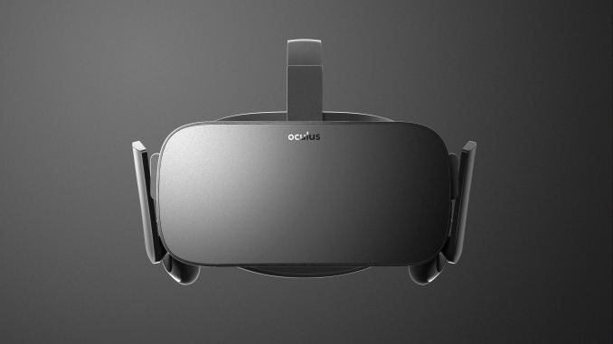

Up until this point, users and developers could buy a development kit with non-final hardware to both test and experiment how to write code and interfaces that can use virtual reality. Oculus will start taking pre-orders for the full retail version later this year. One of the big issues, for me personally, is that VR needs to launch with ground-breaking AAA titles – at least one, if not two. There’s no indication as to what games might be launching in that time, but hopefully they have been working closely with particular game developers to ensure good performance on day one.
At CES this year, when I tested Oculus, hardware specifications were hard to come by. We knew the display was at 90 Hz, requiring a black frame every other frame in order to prevent ghosting. The key take-home message from Brendan Iribe, CEO of Oculus, at the time was that they wanted more. Higher resolution per eye and faster refresh rates were the two key factors, along with what system was powering the content as both of those requirements puts a strain on current graphics solutions. Oculus is set to release details between now and launch, with next week featuring more of the technical specifications.

Brett testing Rift at CES
Pricing is yet unannounced, but other publications have put it in the ‘up to $400’ range, which is similar to the development kits ($350). If I remember correctly, Oculus stated to us in January is that they intent to offer the best VR experience when they launch, and potentially offer partners the chance to create kits themselves but Oculus will always be at the forefront of the technology and software curve in that regard.
Oculus is targeting the Rift at ‘gaming, film, entertainment, communication, and much more’. All angles point to PC content first, although I’m sure that something done with a console can’t be far behind.
PS: In case you missed them, we’ve posted pieces dealing with our hands-on of the Crescent Bay version of the Rift as well as the Vive in recent months.
Read More ...
AMD To Launch New Desktop GPU This Quarter (Q2’15) With HBM
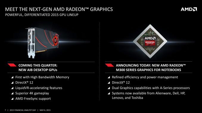
Not mentioned in AMD’s GPU roadmap but now being mentioned by Dr. Su is confirmation that AMD will be launching new desktop GPUs this quarter. AMD is not saying much about these new products quite yet, though based on their description it does sound like we’re looking at high-performance products (and for anyone asking, the picture of the card is a placeholder; AMD doesn’t want to show any pictures of the real product quite yet). These new products will support DirectX 12, though I will caution against confusing that with Feature Level 12_x support until we know more.
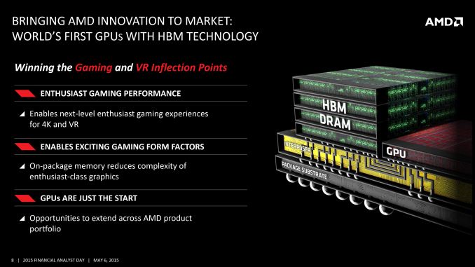
Meanwhile the big news here is that these forthcoming GPUs will be the first AMD GPUs to support High Bandwidth Memory. AMD’s GPU roadmap coyly labels this as a 2016 technology, but in fact it is coming to GPUs in 2015. The advantage of going with HBM at this time is that it will allow AMD to greatly increase their memory bandwidth capabilities while bringing down power consumption. Coupled with the fact that any new GPU from AMD should also include AMD’s latest color compression technology, and the implication is that the effective increase in memory bandwidth should be quite large. For AMD, they see this as being one of the keys of delivering better 4K performance along with better VR performance.
In the process AMD has also confirmed that these HBM-equipped GPUs will allow them to experiment with new form factors. By placing the memory on the same package as the GPU, AMD will be able to save space and produce smaller cards, which will allow them to produce designs other than the traditional large 10”+ cards that are typical of high-end video cards. AMD competitor NVIDIA has been working on HBM as well and has already shown off a test vehicle for one such card design, so we have reason to expect that AMD will be capable of something similar.
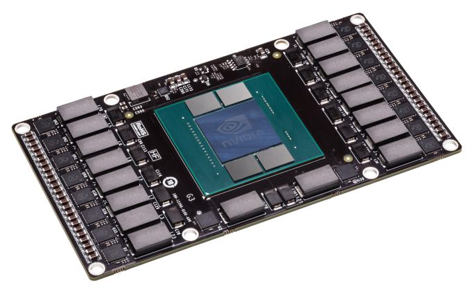
With apologies to AMD: NVIDIA’s Pascal Test Vehicle, An Example Of A Smaller, Non-Traditional Video Card Design
Finally, while talking about HBM on GPUs, AMD is also strongly hinting that they intend to bring HBM to other products as well. Given their product portfolio, we consider this to be a pretty transparent hint that the company wants to build HBM-equipped APUs. AMD’s APUs have traditionally struggled to reach peak performance due to their lack of memory bandwidth – 128-bit DDR3 only goes so far – so HBM would be a natural extension to APUs.
Read More ...
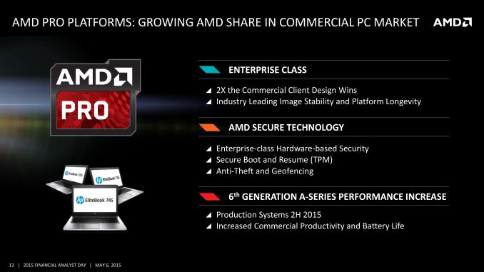
AMD Announces 6th Generation A-Series APU Branding - Carrizo Due This Quarter
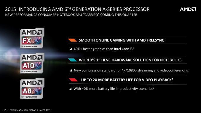
Meanwhile, AMD is also using the opportunity to announce their intended branding for Carrizo notebooks. These products will now be known as the 6th generation A-series, and will be featuring revised AMD badges to indicate this. AMD will be retaining the current FX/A10/A8 branding, with the only real change being the inclusion of the “6th generation” branding on the badges.
Badging aside, AMD still will have to face the fact that they’re launching a 28nm notebook APU versus Intel’s 14nm notebook CPUs, the company is once again banking on their strong GPU performance to help drive sales. Coupled with the combination of low power optimizations in Carrizo and full fixed-function hardware decoding of HEVC, and AMD will be relying on Carrizo to carry them through to 2016 and Zen.
Finally, though it will come a bit later in the year, AMD’s FAD update has also briefly mentioned their plans for their AMD Pro lineup and how Carrizo will impact it. In short, AMD will be leaning on a combination of Carrizo’s power gains, and their own security technology as found in the Pro APUs.
Read More ...
AMD’s 2016-2017 x86 Roadmap: Zen Is In, Skybridge Is Out
The big question on everyone’s mind over the last year has been AMD’s forthcoming x86 Zen CPU, developed by Jim Keller’s group, and Papermaster did not disappoint, opting to address the future of AMD’s x86 plans first and foremost. AMD is not releasing the complete details on Zen until closer to its launch in 2016, but today they are providing some basic details on the CPU’s abilities and their schedule for it.
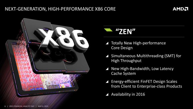
In terms of features, AMD once again confirmed that they’re aiming for significantly higher performance, on the order of a 40% increase in Instruction Per Clock (IPC) throughput. In a significant shift in threading for AMD’s x86 CPUs, Zen will also shift from Bulldozer’s Clustered Multithreading (CMT) to Simultanious Multithreading (SMT, aka Intel’s Hyperthreading). CMT is the basis for Bulldozer’s unusual combination of multiple integer cores sharing a single FPU within a module, so the move to SMT is a more “traditional” design for improving resource usage, and it means Zen will similarly have a more traditional resource layout. AMD is also labeling Zen’s cache as a “high-bandwidth, low latency cache system,” though at this time they aren’t quantifying just how that differs from the Dozer family’s cache.
Meanwhile AMD has confirmed that Zen will be shipping in 2016, and that it will be produced on a yet-to-be-named FinFET process. Our bet would be that AMD continues to use traditional partner (and spin-off fab) GlobalFoundries, who will be ramping up their 14nm equipment for next year as part of their licensing/partnership with Samsung to implement Samsung’s 14nm FinFET process. Zen at this time is AMD’s priority, to the point where the company is willing to push back the ARM K12 in order to get Zen out the door first.
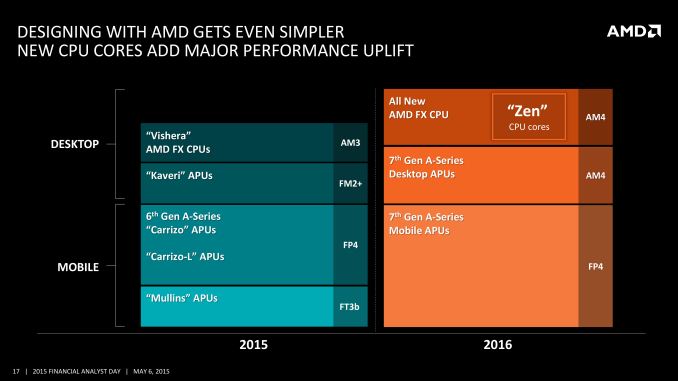
Desktop users will be happy to know that the first Zen processor out the door will be AMD’s high-end desktop CPU (AMD was very deliberate in this, it’s not an APU). AMD will be aiming high and then cascading Zen down into APUs and lower-end products.
Said Zen CPU will use a new AMD platform – AM4 – which will also support DDR4. Unlike the Dozer family, all of AMD’s desktop CPUs will use the same AM4 platform/socket, so when AMD does ramp up their Zen APU, it too will be on AM4 and not its own socket, simplifying the process.
Finally, AMD’s roadmap for Zen over 2016-2017 calls for further improved Zen cores, “Zen+”, later on. Though the biggest jump for AMD comes from the transition from Dozer to Zen, the company is looking to push the envelope on IPC harder than they did with the Dozer family, projecting a higher increase in IPC over time than what we saw with the Dozer parts.

As for what this means for single-threaded performance, that remains to be seen. After having chased a lower-IPC/higher-clockspeed strategy in an attempt to do something different from Intel – the AMD that designed Bulldozer thought it wise not to try to beat well-funded Intel at their own game – the focus on higher IPC is arguably the correct move to make as the laws of physics have continued to keep 5GHz+ clockspeeds from being efficient enough to be practical. That said, single-threaded performance is a combination of IPC and clockspeed, so to be competitive with Intel AMD needs to deliver higher IPC while maintaining relatively high clockspeeds, and the latter is not something AMD is disclosing this early in the process.
Finally, we’ll note that this roadmap is empty of any mentions of project Skybridge. CEO Lisa Su has commented that AMD has decided to change their focus away from Skybridge based on customer feedback. Customers were telling AMD that they didn't necessarily need socket compatible solutions, so AMD is going to work on differentiated solutions. That said, given that Skybridge was announced last year and planned for 20nm, I suspect that it has also become a victim of the short lifespan (and underperforming nature) of 20nm, leading to it being downplayed in favor of 14nm prodcts.
Meanwhile also absent was any further mention of AMD's Cat cores. Zen would appear to be AMD’s top-to-bottom x86 core, a significant departure from an AMD who previously wanted separate designs for the 10W-100W market and sub-10W markets.

Read More ...
AMD’s 2016 GPU Roadmap: FinFET & High Bandwidth Memory

First and foremost, 2016 will be the year of FinFET across AMD, both for the CPU and GPU. Just like Zen, AMD will have GPUs on an unnamed FinFET process in 2016. AMD isn’t saying much else about 2016 at this point in terms of chips or architecture, but they are saying that the combination of the 2016 architecture and the use of FinFET will result in a 2x improvement in energy efficiency over what AMD is calling their “previous generation GPU” (though it’s not clear if it’s relative to an existing GPU or something else due in 2015). Based on AMD’s comments, it sounds like the majority of these gains will come from the use of the newer manufacturing process, as opposed to architectural efficiency gains. AMD is also mum on which fab will be building this GPU, however the timeframe is such that it lines up with TSMC’s 16nm FinFET plans, with TSMC being AMD’s traditional fab of choice for GPUs.
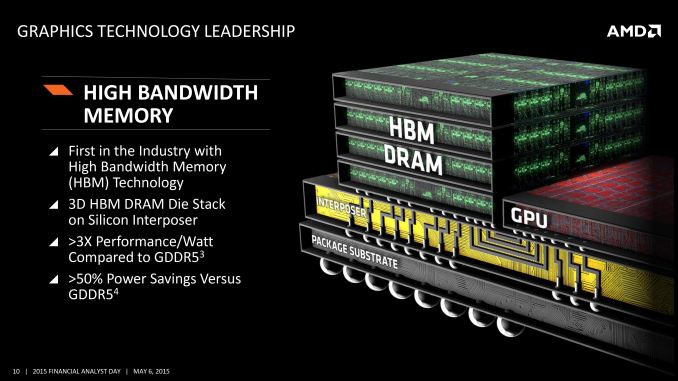
Meanwhile after the circulation of a number of rumors, AMD has confirmed that they will be shipping GPUs with High Bandwidth Memory (HBM) technology. HBM involves stacking DRAM dies on top of each other, and then locating them next to or on top of a processor, the close proximity allowing for a very wide, very high bandwidth memory bus. AMD isn’t saying what absolute performance is like at this time, but HBM should better than triple their memory perf-per-watt compared to GDDR5, with a better than 50% reduction in power consumption.
AMD’s roadmap and diagrams also make it clear that we’re looking at a 2.5D solution; that is, HBM RAM stacks organized around a processor rather than on top of it. These stacks are then routed to the processor based on an interposer layer that both the RAM stacks and processor sit in, and the interposer itself sits above the traditional package substrate. Given the high thermal output of high-end GPUs, this is what we’d expect as putting RAM on top of the GPU would make it that much harder to cool.
Finally, AMD is stating that they expect to be the first vendor to deploy HBM, meaning that we’re looking at a launch of an HBM-equipped video card sooner than NVIDIA’s Pascal, which was previously announced to be using the same technology.

Read More ...
AMD’s K12 ARM CPU Now In 2017
AMD’s “Seattle” SoC – the ARM Cortex-A57 powered Opteron A1100 – will finally be shipping in H2 of this year, after first sampling towards the end of last year. This unfortunately is almost a year behind AMD’s original schedule, though AMD seems moderately optimistic about catching up once they have their first ARM silicon out the door.
But the real focus of AMD’s comments on ARM for FAD involve K12, the AMD-developed ARM CPU core being designed alongside Zen. With AMD having opted to prioritize Zen development, K12 has been pushed back from 2016 to 2017, essentially taking the near-simultaneous launch of the two parts off the table. AMD for their part is attributing this change in schedule only to the decision to focus on Zen, however with Opteron A1100 delayed, it’s entirely possible this is also a knock-on effect that has pushed back the entire AMD ARM roadmap.
In any case, even with the delay AMD is still eagerly moving ahead with their ARM plans. A1100, even though it’s late, will be the pathfinder for AMD’s ARM efforts, serving as a platform to further develop the AMD ARM ecosystem, getting developers acquainted with the technology and getting software ready for it. K12 in turn will come in after that ecosystem has already seen some development, allowing AMD to get their new hardware out to the market and already have software support for it. I hesitate to say that this makes A1100 entirely a pathfinder product – until it’s available, it’s not clear how many customers might purchase it for production work – but clearly AMD’s big play is K12, not A1100.
And though K12 is delayed, AMD tells us that this hasn’t changed how it’s being developed, which is to say that it’s being done in concert with Zen. So virtually everything AMD gets right with Zen will be integrated into K12 as well, just on the basis of the ARM ISA instead of x86. AMD still believes that the time is right for ARM in the server space – along with a very obvious place in the semi-custom SoC space – and that K12 will be an interesting alternative to Zen in that regard.
Read More ...
AMD Charts Future Growth Opportunities
The last time AMD held a FAD was in 2012. In the intervening years the company has undergone a number of changes for both the good and the bad, including the major console wins, continued struggles with PC market share, and of course a change in leadership from Rory Read to Dr. Lisa Su. Today’s FAD in turn is a chance for Dr. Su to show in greater detail her plans for the company, and where those plans will take AMD in the next couple of years.

AMD’s kicking off today’s FAD with a quick overview of what they see as the company’s major growth opportunities: gaming, immersive platforms, and the datacenter.
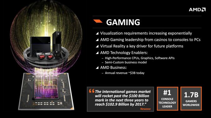
AMD of course is no stranger to gaming – they already attribute ~$3 billion in revenue to it – but AMD believes further growth is possible. They have a strong graphics IP portfolio, powerful silicon, and they are already in everything from casinos to high-end PCs, and everything in between. AMD is banking particularly hard on virtual reality through technologies such as LiquidVR, a somewhat risky affair (ask TV manufacturers about 3D TVs), but one that can potentially pay off well due to the high system requirements of VR.
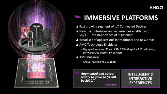
AMD believes their second growth opportunity is immersive platforms, which is sort of a catch-all for everything from IoT to VR; essentially anything with a more “personal” connection to the user than traditional PCs and mobile devices. This broad category means leveraging virtually the entire company, CPU and GPU side, x86 and ARM.
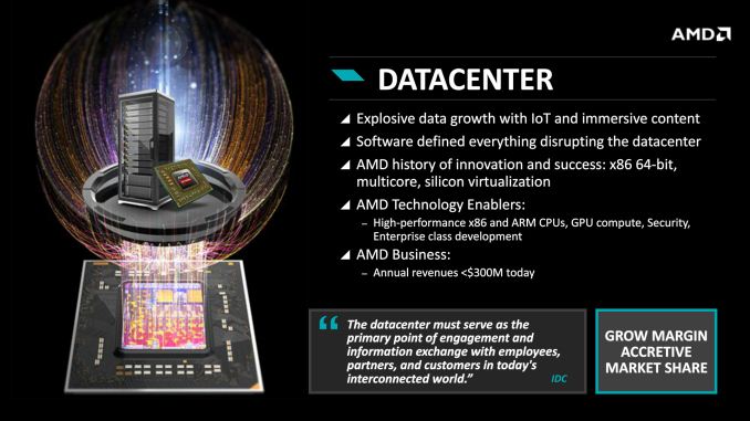
Last but not least, AMD considers datacenters to be their final opportunity for growth. After a solid run with the Opteron series and AMD’s jump on 64-bit computing, the company has become increasingly locked out of the server and datacenter market – revenues from it are under $300M these days – and they’re looking to get back in. A lot of this will be driven by technology, with AMD relying on their future Zen (x86) and K12 (ARM) CPUs to help improve their competitive positioning, along with some good old fashioned pragmatism in as much as AMD intends to take advantage of the shift to server-side/cloud computing.
Overall, none of the growth opportunities here are surprising given what AMD has been saying in the past. Whereas FAD 2012 marked AMD’s intention to shift from being almost entirely PC focused towards being ambidextrous and leveraging semi-custom silicon, FAD 2015 presents AMD as continuing to chase many of those same opportunities which they have already been chasing for the last year or more. Ultimately the key to AMD’s growth plans will rely on correctly predicting what opportunities they need to follow to grow – particularly rapidly expanding markets as opposed to stealing revenue from existing players – and then executing on that in a timely manner with solid hardware.

Read More ...
The Lenovo ThinkStation P900 Workstation Review: Design 101
The workstation market has always been a consistent seller. The dream of offloading to an on or off-site VM and a cluster for work processing still lies more in the realm of mass production over local quick-to-compute work, and because of that low latency for quick interaction, workstations are here to stay. While the consumer is going smaller, business aims to scale and on the back of our P300 review, Lenovo sent their 34kg dual Xeon E5 v3 behemoth version of the ThinkStation P900 for review.
Read More ...
Leak Shows Possible Super Sentinel Spy Drone Receiving a Boom In-Air Refuel
This new "Super Sentinel" could stay aloft for weeks with help from local fuel tankers
Read More ...
Report: Xbox One Gets DVR Functionality, in Media Center Replacement Bid
Meanwhile Microsoft confirms the death of Windows Media Center, confirms DVD playback functionality will be replaced
Read More ...
Rombertik is a Bizarre, Scary Brilliant Piece of Self-Destructing Malware
While its chief goal is to watch your web traffic, it goes about that goal in remarkable fashion
Read More ...
Available Tags:AMD , Radeon , Notebook , GPU , APU , CPU , Lenovo , Xbox ,
No comments:
Post a Comment