
NVIDIA’s GRID Game Streaming Service Rolls Out 1080p60 Support

Today’s announcement from NVIDIA comes as the company is ramping up for the launch of the SHIELD Android TV and its accompanying commercial GRID service. The new SHIELD console is scheduled to ship this month, meanwhile the commercialization of the GRID service is expected to take place in June, with the current free GRID service for existing SHIELD portable/tablet users listed as running through June 30th. Given NVIDIA’s ambitions to begin charging for the service, it was only a matter of time until the company began offering the service, especially as the SHIELD Android TV will be hooked up to much larger screens where the limits of 720p would be more easily noticed.
In any case, from a technical perspective NVIDIA has long had the tools necessary to support 1080p streaming – NVIDIA’s video cards already support 1080p60 streaming to SHIELD devices via GameStream – so the big news here is that NVIDIA has finally flipped the switch with their servers and clients. Though given the fact that 1080p is 2.25x as many pixels as 720p, I’m curious whether part of this process has involved NVIDIA adding some faster GRID K520 cards (GK104) to their server clusters, as the lower-end GRID K340 cards (GK107) don’t offer quite the throughput or VRAM one traditionally needs for 1080p at 60fps.
But the truly difficult part of this rollout is on the bandwidth side. With SHIELD 720p streaming already requiring 5-10Mbps of bandwidth and NVIDIA opting for quality over efficiency on the 1080p service, the client bandwidth requirements for the 1080p service are enormous. 1080p GRID will require a 30Mbps connection, with NVIDIA recommending users have a 50Mbps connection to keep from any other network devices compromising the game stream. To put this in perspective, no video streaming service hits 30Mbps, and in fact Blu-Ray itself tops out at 48Mbps for audio + video. NVIDIA in turn needs to run at a fairly high bitrate to make up for the fact that they have to all of this encoding in real-time with low latency (as opposed to highly optimized offline encoding), hence the significant bandwidth requirement. Meanwhile 50Mbps+ service in North America is still fairly rare – these requirements all but limit it to cable and fiber customers – so at least for now only a limited number of people will have the means to take advantage of the higher resolution.
| NVIDIA GRID System Requirements | ||
| 720p60 | 1080p60 | |
| Minimum Bandwidth | 10Mbps | 30Mbps |
| Recommended Bandwidth | N/A | 50Mbps |
| Device | Any SHIELD, Native Or Console Mode | Any SHIELD, Console Mode Only (no 1080p60 to Tablet's screen) |
As for the games that support 1080p streaming, most, but not all GRID games support it at this time. NVIDIA’s announcement says that 35 games support 1080p, with this being out of a library of more than 50 games. Meanwhile I’m curious just what kind of graphics settings NVIDIA is using for some of these games. With NVIDIA’s top GRID card being the equivalent of an underclocked GTX 680, older games shouldn’t be an issue, but more cutting edge games almost certainly require tradeoffs to maintain framerates near 60fps. So I don’t imagine NVIDIA is able to run every last game with all of their settings turned up to maximum.
Finally, NVIDIA’s press release also notes that the company has brought additional datacenters online, again presumably in anticipation of the commercial service launch. A Southwest US datacenter is now available, and a datacenter in Central Europe is said to be available later this month. This brings NVIDIA’s total datacenter count up to six: USA Northwest, USA Southwest, USA East Coast, Northern Europe, Central Europe, and Asia Pacific.
Read More ...
Avago Announces PLX PEX9700 Series PCIe Switches: Focusing on Data Center and Racks

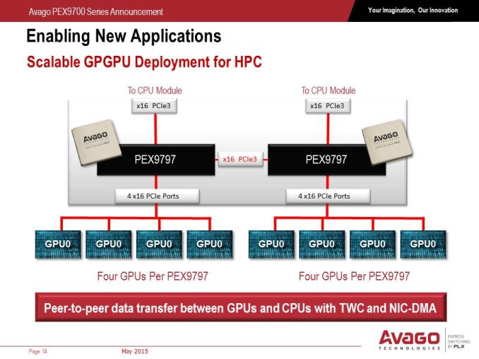
Today’s announcement is from Avago, the company that purchased PLX back in June 2014, for a new range of PCIe switches focused on the data center and racks called the PEX9700 series. Part of the iterative improvements in PCIe switches should ultimately be latency and bandwidth, but there are several other features worth noting which from the outside might not be considered, such as the creation of a switching fabric.
Typically the PCIe switches we encounter in the consumer space use one upstream host to several downstream ports, and each port can have a series of PCIe lanes as bandwidth (so 4 ports can total 16 lanes, etc). This means there is one CPU host by which the PCIe switch can send the work from the downstream ports. The PLX9700 series is designed to communicate with several hosts at once, up to 24 at a time, allowing direct PCIe to PCIe communication, direct memory copy from one host to another, or shared downstream ports. Typically PCIe is a host-to-device topology, however the PEX9700 line allows multiple hosts to come together with an embedded DMA engine on each port to probe host memory for efficient transfer.
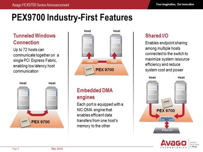
Unlike the previous PCIe switches from PLX, the new series also allows for downstream port isolation or containment, meaning that if one device downstream fails, the switch can isolate the data pathway and disable it until it is replaced. This can also be done manually as the PEX9700 series will also come with a management port which Avago states will use software modules for different control applications.
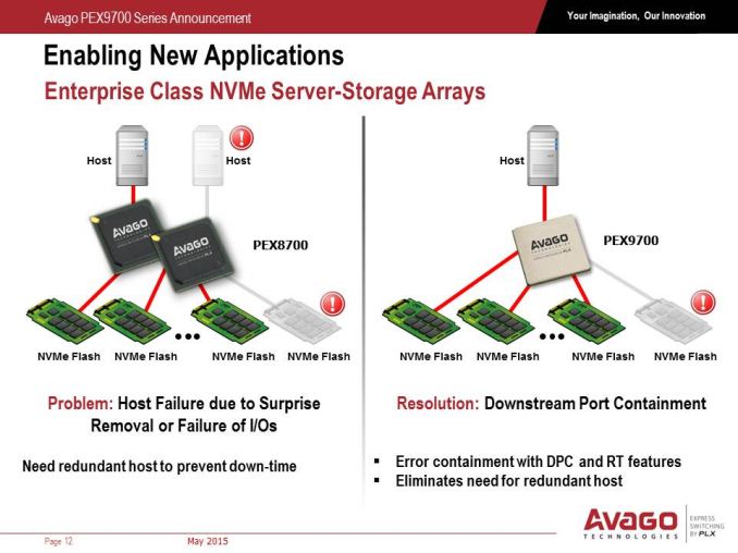
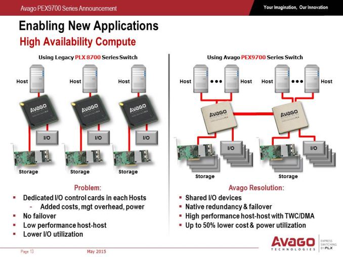
In the datacenter and within rack infrastructure, redundancy is a key feature to consider. As the PEX9700 switches allow host-to-host communication, it also allows control from multiple hosts, allowing one host to take over in the event of failure. The switches can also agglomerate and talk to each other, allowing for multiple execution routes especially with shared IO devices or in multiple socket systems for GPGPU use. Each switch will also have a level of hot-plugging and redundancy, allowing disabled devices to be removed, replaced and restarted. When it comes to IO, read requests mid-flow are fed back to the host as information on failed attempts, allowing instant reattempts when a replacement device is placed back into the system.
Avago is stating that the 9700 series will have seven products ranging from 5 to 24 ports (plus one for a management port) from 12 to 97 lanes. This also includes hot plug capability, tunneled connections, clock isolation and as mentioned before, downstream port isolation. These models are currently in full scale production, as per today’s announcement, using TSMC's 40nm process. In a briefing call today with Akber Kazmi, the Senior Product Line Manager for the PEX9700 series, he stated that validation of the designs took the best part of eight months, but that relevant tier one customers already have their hands on the silicon to develop their platforms.
For a lot of home users, this doesn’t mean that much. We might see one of these switches in a future consumer motherboard focused on dual-socket GPGPU, but the heart of these features lies in the ability to have multiple nodes access data quickly within a specific framework without having to invest in expensive technologies such as Infiniband. Avago is stating a 150ns latency per hop, with bandwidth limited ultimately by the upstream data path – the PCIe switch ultimately moves the bandwidth around to where it is most needed depending on downstream demand. The PEX9700 switches also allow for direct daisy chaining or as a cascading architecture through a backplane, reducing costs of big switches and allowing for a peak bandwidth between two switches of a full PCIe 3.0 x16 interface, allowing scaling up to 128 Gbps (minus overhead).
Personally, the GPGPU situation interests me a lot. When we have a dual socket system with each socket feeding multiple GPUs, with one PEX9700 switch per CPU (in this case, PEX9797) but interconnected, it allows GPUs on one socket to talk to GPUs on the other without having to go all the way back up to the CPU and across the QPI bus, which saves both latency and bandwidth, and each of the PCIe switches can be controlled.
The PEX9700 series of switches bucks the status quo of requiring translation layers such as NICs or Infiniband for host-to-host-to-device communication and all inbetween, which is what Avago is hoping the product stack will accomplish. The main factors that Avago see the benefit include latency (fewer translation layers for communication), cost (scales up to 128 Gbps minus overhead), power (one PEX9700 chip has a 3W-25W power rating) and energy cost savings on top of that. On paper at least, the capabilities of the new range could potentially be disruptive. Hopefully we'll get to see one in the flesh at Computex from Avago's partners, and we'll update you when we do.
Source: Avago


Read More ...
The AMD A8-7650K APU Review, Also New Testing Methodology
The staggered birth of Kaveri has been an interesting story to cover but it has been difficult to keep all the pieces right in the forefront of memory. The initial launch in January 2014 saw a small number of SKUs such as the A10-7850K and the A8-7600 at first and since then we have had a small trickle at a rate of one or two new models a quarter hitting the shelves. We've seen 65W SKUs, such as in the form of the A10-7800, which offer 45W modes as well. Today we're reviewing the most recent Kaveri processor to hit the market, the A8-7650K rated at 95W and officially priced at $105/$95.
Read More ...
AMD’s Carrizo-L APUs Unveiled: 12-25W Quad Core Puma+
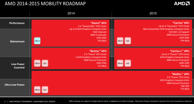
Carrizo-L features ‘Puma+’, which by virtue of the naming scheme suggests an updated version of Puma which was seen in Beema. What the ‘plus’ part of the name means has not been disclosed, as both Puma and Puma+ are reported to be 28nm, but chances are that the design has attacked the low hanging fruit in the processor design, rather than purely just a frequency bump. Carrizo-L will be advertised under the new ‘AMD 7000 Series’ APUs, featuring up to four low power separate cores up to 2.5GHz, up to 25W and up to DDR3-1866 support. These are aimed square at the Atom ecosystem within a similar power budget.
| AMD Carrizo-L | |||||
| A8-7410 | A6-7310 | A4-7210 | E2-7110 | E1-7010 | |
| Cores / Threads | 4 / 4 | 4 / 4 | 4 / 4 | 4 / 4 | 2 / 2 |
| CPU Frequency | Up to 2.5 GHz | Up to 2.4 GHz | Up to 2.2 GHz | Up to 1.8 GHz | Up to 1.5 GHz |
| TDP | 12-25W | 12-25W | 12-25W | 12-15W | 10W |
| L2 Cache | 2MB | 2MB | 2MB | 2MB | 1MB |
| DRAM Frequency | DDR3L-1866 | DDR3L-1600 | DDR3L-1600 | DDR3L-1600 | DDR3L-1333 |
| Radeon Graphics | R5 | R4 | R3 | 'Radeon' | 'Radeon' |
| Streaming Processors | 128 ? | 128 ? | 128 ? | 128 ? | 128 ? |
| GPU Frequency | Unknown | Unknown | Unknown | Unknown | Unknown |
AMD is stating that these APUs are currently available in Greater China already with a global rollout commencing in due course. All APUs are listed with AMD Radeon graphics, although the Rx number has no indication as to the streaming processors in the graphics part – a similar situation happened with Beema, and all those parts came with 128 SPs, differing only in frequency which is likely the case here. The SoC design also ensures all the IO is onboard, including an AMD Secure Processor, which for Puma was a Cortex-A5 supporting ARM TrustZone. It is likely that Carrizo-L also uses only a single memory channel, similar to Beema.
One of the more interesting elements is that Carrizo and Carrizo-L will share a socket, known as FP4. This means the processors are pin compatible, and what we know about Carrizo at this point suggests that both segments will play within the same sort of power budget (10-25W vs 15-35W). This allows OEMs to build two designs with almost identical hardware under the hood except for the SoC – would you prefer a single/dual Excavator design, or a faster frequency quad-core Puma+ design? There also leaves scope for differential integrated graphics performance, as mobile Kaveri up to 25W had up to 384 SPs or 3x what we are expecting with Carrizo-L. A lot of the performance metrics in this part will be down to binning the various designs, which adjusts the cost.
At some point we will source a Carrizo-L low-power notebook in order to test the hardware – it would be an interesting data point to get a corresponding Carrizo design as well.
Source: AMD
Read More ...
MediaTek Unveils Helio X20 Tri-Cluster 10-Core SoC

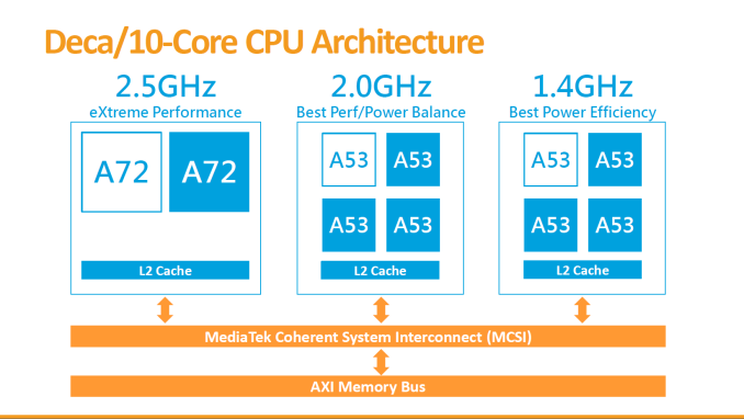
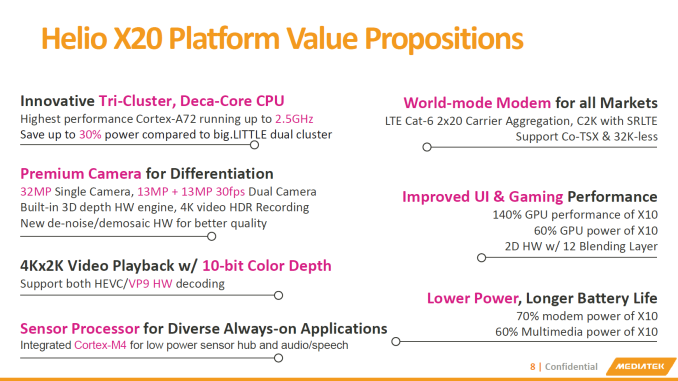
Right off the bat, MediaTek manages to raise eyebrows with what is the first 10 core System-on-a-Chip design. The 10 processor cores are arranged in a tri-cluster orientation, which is a new facet against a myriad of dual-cluster big.LITTLE heterogeneous CPU designs. The three clusters consist of a low power quad-core A53 cluster clocked at 1.4 GHz, a power/performance balanced quad-core A53 cluster at 2.0GHz, and an extreme performance dual-core A72 cluster clocked in at 2.5GHz. To achieve this tri-cluster design, MediaTek chose to employ a custom interconnect IP called the MediaTek Coherent System Interconnect (MCSI).
We'll get back to the new innovative CPU arrangement in a bit, but first let's see an overview of what the rest of SoC offers. MediaTek is proud to present its first CDMA2000 compatible integrated modem with the X20. This is an important stepping stone as the company attempts to enter the US market and try to breach Qualcomm's stronghold on the North American modems and SoCs. Besides C2K, the X20's modem allows for LTE Release 11 Category 6 with 20+20MHz Carrier Aggregation (downstream), supporting speeds up to 300Mbps in the downstream direction and 50Mbps upstream. The new modem also is supposed to use 30% less power when compared to the Helio X10.
The SoC also has an integrated 802.11ac Wi-Fi with what seems to be a single spatial stream rated in the spec sheets up to 280Mbps.
| MediaTek Helio X20 vs The Competition | ||||
| SoC | MediaTek Helio X20 (MT6797) |
MediaTek Helio X10 (MT6795) |
Qualcomm Snapdragon 808 (MSM8992) |
Qualcomm Snapdragon 620 (MSM8976) |
| CPU | 4x Cortex A53 @1.4GHz 4x Cortex A53 @2.0GHz 2x Cortex A72 @2.3-2.5GHz |
4x Cortex A53 @2.2GHz 4x Cortex A53 @2.2GHz |
4x Cortex A53 @1.44GHz 2x Cortex A57 @1.82GHz |
4x Cortex A53 @1.2GHz 4x Cortex A72 @1.8GHz |
| Memory Controller |
2x 32-bit @ 933MHz LPDDR3 14.9GB/s b/w |
2x 32-bit @ 933MHz LPDDR3 14.9GB/s b/w |
2x 32-bit @ 933MHz LPDDR3 14.9GB/s b/w |
2x 32-bit @ 933MHz LPDDR3 14.9GB/s b/w |
| GPU | Mali T8??MP4 @700MHz |
PowerVR G6200 @700MHz |
Adreno 418 @600MHz |
"Next-gen" Adreno |
| Encode/ Decode |
2160p30 10-bit H.264/HEVC/VP9 decode 2160p30 HEVC w/HDR encode |
2160p30 10-bit H.264/HEVC/VP9 decode 2160p30 HEVC encode |
2160p30, 1080p120 H.264 & HEVC decode 2160p30, 1080p120 H.264 encode |
2160p30, 1080p120 H.264 & HEVC |
| Camera/ISP | Dual ISP 32MP @ 24fps |
13MP | Dual ISP 21MP |
Dual ISP 21MP |
| Integrated Modem |
LTE Cat. 6 300Mbps DL 50Mbps UL 2x20MHz C.A. (DL) |
LTE Cat. 4 150Mbps DL 50Mbps UL |
"X10 LTE" Cat. 9 450Mbps DL 50Mbps UL 3x20MHz C.A. (DL) |
"X8 LTE" Cat. 7 300Mbps DL 100Mbps UL 2x20MHz C.A. (DL & UL) |
Video encoding and decoding capabilities seem to be carried over from the MT6795 / X10, but MediaTek advertises a 30% and 40% improvement in decoding and encoding power consumption respectively.
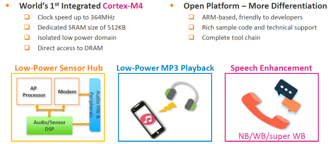
Still on the multimedia side, we see the employment of a new integrated Cortex-M4 companion-core which serves as both an audio processor for low-power audio decoding, speech enhancement features and voice recognition, as well as sensor-hub function acting as a microcontroller for offloading sensor data processing from the main CPU cores. This means that while the device has the display turned off but is playing audio, only the M4 is in use in order to prolong battery life.
On the GPU side, the X20 seemed to be the first officially announced Mali T800 series GPU SoC. MediaTek explains that this is a still-unreleased ARM Mali high-end GPU similar to the T880. MediaTek initially chose a more conservative MP4 configuration clocked in at 700MHz, although final specifications are being withheld at this time. It should be noted that Mediatek has traditionally never aimed very high in terms of GPU configurations. It could be considered that the GPU in the X20 could still remain competitive in prolonged sustained loads as we saw larger Mali implementations such as Samsung's Exynos SoCs not being able to remain in the thermal envelope at their maximum rated frequencies. Initial relative estimates of the X20, expressed by MediaTek, compared to the Helio X10's G6200 see a 40% improvement in performance with a 40% drop in power.
On the memory side, MediaTek remains with a 2x32bit LPDDR3 memory interface running at 933MHz. MediaTek reasons that the SoC is limited to 1440p devices and the LPDDR3 memory should be plenty enough to satisfy the SoC's bandwidth requirements (a notion I agree with, given the GPU configuration).
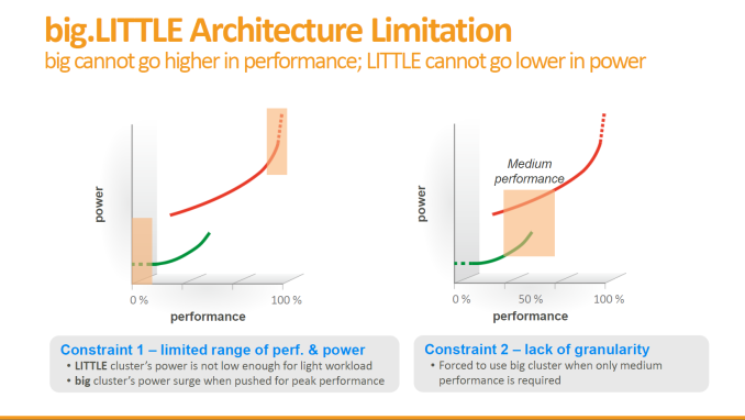
Going back to the signature 10-Core/Tri-Cluster architecture of the SoC, MediaTek explains that this was a choice of power optimization over conventional two-cluster big.LITTLE designs. b.L works by employing heterogeneous CPU clusters - these may differ in architecture, but can also be identical architectures which then differ in their electrical characteristics and their target operating speeds. We've covered how power consumption curves behave in our Exynos 5433 deep-dive, and MediaTek presents a similar overview when explaining the X20's architecture.
One option in the traditional 2-cluster designs is to employ a low-power low-performance cluster, typically always a lower-power in-order CPU architecture such as ARM's A53. This is paired with a higher-power high-performance cluster, either a larger CPU core such as the A57/A72, or a frequency optimized A53 as we see employed in some past MediaTek SoCs, or most recently, HiSilicon's Kirin 930 found in the Huawei P8.
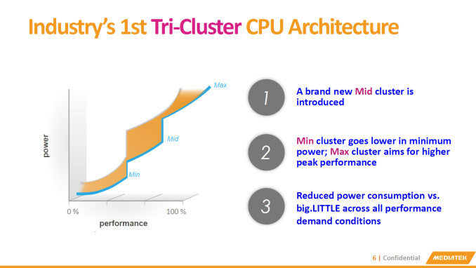
Contrary to what MediaTek presents as an "introduction of a Mid cluster", I like to see MediaTek's tri-cluster approach as an extension to the existing dual A53 cluster designs - where the added A72 cluster is truly optimized for only the highest frequencies. Indeed, we are told that the A72 cluster can reach up to 2.5GHz on a TSMC 20nm process. ARM aims similar clocks for the A72 but at only 14/16nm FinFET processes, so to see MediaTek go this high on 20nm is impressive, even if it's only a two-core cluster. It will be interesting to see how MediaTek chooses the lower frequency limits on each cluster, especially the A72 CPUs, or how these options will be presented to OEMs.
The end-result is a promised 30% improvement in power consumption over a similar 2-cluster approach. This happens thanks to the finer granularity in the performance/power curve and an increase in available performance-power points for the scheduler to place a thread on. Having a process that is heavy enough that it is not capable of residing on the smallest cluster due to performance constraints, but not demanding enough to require the big cluster's full performance, can now reside on this medium cluster at much greater efficiency than had it been running on the big cluster at reduced clocks. MediaTek uses CorePilot as a custom developed scheduler implementation that is both power aware and very advanced (based on our internal testing of other MediaTek SoCs). My experience and research with it on existing devices was fairly positive, so I'm sure the X20's new v3.0 implementation of CorePilot will be able to take good advantage of the tri-cluster design.
The biggest question and need of clarification is in the area of what the MCSI (the interconnect) is capable of. ARM had announced its CCI-500 interconnect back in February, which incidentally also promised the capability of up to 4 CPU clusters. MediaTek hinted that this may be a design based on ARM's CCI - but we're still not sure if this means a loosely based design or a direct improvement of ARM's IP. Cache coherence is a major design effort, and if MediaTek saw this custom IP as an effort worth committing to, then the MCSI may have some improvements we're still not clear on.
The Helio X20 is certainly an interesting SoC and I'm eager on how the tri-cluster design performs in practice. The X20 samples in H2 2015 and devices with it are planned to be shipping in Q1 2016. In the given time-frame, it seems the X20's primary competitor is Qualcomm's Snapdragon 620, so it'll be definitely a battle for the "super-mid" (as MediaTek likes to put it) crown.
Read More ...
Early Yahoo Executive, YouTube Development Chief, Venkat Panchapakesan, Dies
Venkat Panchapakesan will be missed but his legacy lives on
Read More ...
No Matter What the AP Tells You, Google's Self-Driving Cars are Pretty Safe
While recent report dwells on sensationalist hypotheticals regarding pedestrian collisions, the facts speak to a different truth
Read More ...
Available Tags:AMD , APU , Yahoo , YouTube ,
No comments:
Post a Comment