
GIGABYTE AM1M-S2H Review: What Can $35 Get You?
While most of the time enthusiasts are playing around with the latest and greatest, the cheaper low performance platforms are usually the high volume movers. As we explained in our Kabini review, AMD has taken the unusual step of producing an upgradable platform for as little as $74. The motherboards for the AM1 Kabini platform range from $31 to $47, and today we are reviewing the GIGABYTE AM1M-S2H which retails at $35.
Read More ...
ASUS Motherboard Division Director: An Interview with Dr Albert Chang

Ian Cutress: Everyone sees a corporation, but there are always interesting people to talk to. Everyone has a back story and it is always interesting to hear how people have risen to where they are. Your business card says ‘Division Director’ – what exactly does a Division Director do?
Albert Chang: I am the ASUS motherboard R&D head, so I have three major teams. One of these is in Taiwan, with two others in China. The team in Taiwan focuses on ROG, with the other two in China for channel motherboards and SI customer designs.
IC: What is your typical day?
AC: Usually I have to review all the projects. We usually have 20-30 projects running at the same time. Being one person it can be hard to review all details, but I have staff that report to me and then I can discuss any problems in case any department needs assistance or approval.
IC: How long have you been in this position at ASUS?
AC: I have been Division Director for two years and at ASUS since 2002 straight after finishing my PhD from the National Taiwan University. I started as an engineer, checking datasheets and layouts. At ASUS, as a motherboard engineer, you are the project owner and you have to discuss everything with the Product Manager (layout, engineering) and others like the power and layout engineers. We had to design based on the specification sheets and confirm with layout engineers. I managed a couple of people at that time, and a lot more now!
IC: With regards to your education, what were your courses?
AC: I majored in Electrical Engineering, with a focus on Power Electronics. I finished my PhD at 28 and joined ASUS at that time.
IC: In your position, do you work a ‘9-to-5’, or do you have to come in on weekends?
AC: Sometimes at weekends, especially to have meetings with either North America or Europe, or to fix major issues that rise up. I have a family, but they are not too keen on me coming in on weekends! I sometimes have to buy cake or a gift when I get home!
IC: As Division Director, do you get final say on what happens with the motherboards?
AC: On the engineering side, yes, but there are also the firmware and software teams.
IC: Does the sales department ask you to do certain designs?
AC: All requests of that nature go through the product managers, who relay information through to R&D. So for ROG, Kris Huang (we interviewed him in 2012) is the product manager.
IC: How does user demand get fed back into designs?
AC: Typically I will speak to our product managers (both sales and marketing), or our technical marketing teams directly who monitor the forums and produce reports about user experience. Sometimes I like to hear direct from the teams gathering this information and interacting directly with the users, especially with our major regions such as North America. We have to look at the global market, and decide on ideas or features that benefit everyone.
IC: In terms of ideas for future platforms, who gets them/where do they come from?
AC: We initially look at our competitors’ product, to see which direction they are going, and also examine media reviews to see which options they like or want to see improved. Features like the OC Panel come from the engineers in the ROG team. Because I am only one person, we encourage every engineer to share any ideas in meetings so we can discuss them. There are multiple streams – some from in-house engineers, some from feedback, and some from product managers.
IC: What percentage of users need to request a feature before it is implemented?
AC: If a request comes up repeatedly, we evaluate the idea based on relevance and increased cost on the motherboards. For example, adding DC and PWM fan control on the motherboard came from a core group of users that wanted to be able to have the control. It also helps if the media notice the new feature as well, and can help relay this to other users.
IC: How is market research for new ideas performed?
AC: We have the forums, but also social media plays a role. We sometimes give users a choice between two features (for example, audio codec A or B), and even if we only get 40 or so responses, we weigh up the percentages. The product managers for each region that understand their customers can also have input on new ideas.
IC: At what point in the product cycle to you start looking at the next generation of motherboards? If you released a motherboard today, how far back would you have to start planning for it?
AC: At least nine months, in terms of the start point in thinking about what we want to do.
In the first three months, we will start analyzing the new major features for the CPU and chipset generation from the CPU manufacturer guidelines, paying attention to the differences to the old platform. We also look over bugs from the old generation, or ideas that we could not implement in the last generation. We also check the competitors’ products for the last generation, including the feedback from their users. At that point we talk to the major IC vendors (Renesas, ASMedia, Qualcomm Atheros) for their plans and roadmaps for the next 6-9 months so we have the latest for launch.
In month four, we finalize the segmentation for the product line, including form factor, and start the circuit design. We also work with Intel with early samples which can have a lot of bugs, so we report back to Intel in terms of processor and chipset evaluation for their PVT/first stepping samples. The microcode gets revised several times. We take 4-6 weeks for the circuit design before we get the first motherboards ready for testing, and by this time we have those Intel CPU samples for testing.
We build 60-100 boards for a sample run when the design is coming together, for validation, reliability, checking the power and everything. This includes the aging tests, such as high temperature stress testing. Typically our rule is a 12 hour test at this point, and if there are any errors in those twelve hours for these pre-production models, we then have to check it. The process of testing, changing and retesting can take up to three months to catch any bugs. At every change or iteration due to hardware bugs, we need to retest and revalidate.
At 7.5 months, we are at PVT stage before mass production. We ensure all the third party IC orders are in and will work with the motherboards. We work with factories in China for mass production and place our orders with them to build our motherboards. We have to check the production quality of the factory output. We typically send project managers or leaders to manage production and work with the factories in terms of managing the schedules as well as quantity.
Mass production starts about a month before launch, and in that time we also distribute hardware around the world. This also involves the sales teams talking to their local regional SIs, as well as inviting media to preview events. Typically the media receive samples from the first mass production batch.
IC: So by the timeline, users and media need to start asking for certain features around 5-8 months before a launch! We normally do not know that there is a launch until it almost happens.
AC: Yes, sometimes changes late in the day are difficult to do. But we keep the ideas generated throughout the generation and see what we can apply next time around. But for example, with the memory design, we do not always follow Intel guidelines. We have our own memory team and do a lot of simulations based on layout and tracing to find the best way to get the most out of the memory. We want to better than the reference design, and ROG team is the best at pushing the new designs. So if we want the best memory records, we need to have the best design.
IC: How long is the lead time, from placing an order to receiving stock, for the controllers?
AC: For the testing motherboards, we usually can get stock within a week or two. For the mass production, if it works in our design, it is more like 4-6 weeks. This includes other things like the PCB, which can sometimes be over 6 weeks.
IC: When do you start designing the additional materials (box, foam inserts, manuals)?
AC: We go through a lot of internal discussions, and there are a lot of revisions when it comes down to design. The design teams talk to sales and see what the competition are doing, but early design talks can be 6-9 months away from a launch, as the tracing teams are designing the motherboards.
IC: When you mention 60-100 motherboards for a sample run, is that 100 motherboards for every SKU? So for the seven Z97 channel motherboards, you would have almost 700 samples?
AC: Yes, every SKU, of course!
IC: In terms of product production goals, what would be your main goals in the next twelve months?
AC: In the first two months of a launch, we check to see if our features meet the customers’ needs. After that, we start to study the next generation. For me, I hope that each generation we can make the boards that everyone likes, because this is my product line at ASUS.
IC: How about the next five years?
AC: I will still be at ASUS, and I want to help expand PC applications in the home. Our chairman Jonney Shih has mentioned at Computex that this is a primary focus for ASUS.
IC: What do you think are the most important innovations that ASUS has created in the motherboard segment recently?
AC: Too many, cannot pick! Our ROG features span so many projects, for example. We have made our overclocking features easier to use than before, especially with automatic overclocking in BIOS and software, but also with the ROG OC Panel. Not many users know how to overclock, so we want to make it easier with our Auto Tuning, especially with voltages and stress testing. But we also cater for the extreme tweakers that use ROG.
IC: What element or feature from the ASUS Motherboard Business Unit do you think users need to know more about?
AC: We use separate components on the motherboard to help manage features like overclocking, but not many users know that we also do the same for other features like power saving. This is separate from the CPU and chipset, for example our Dual Intelligent Processors design. This is our own custom designed chip for our motherboards, not something off the shelf, which users may not realize.
IC: Do you see a gap in the market that ASUS or the Motherboard Business Unit should move in to?
AC: Gaming and small form factor markets are growing, and other ultra-small form factors like the NUC and Chromebox are interesting. We announced the GR8 at Computex, which is a combination of this for around 1.5 liter of volume. The sub 1-liter market should be a focus in the future.
IC: A question I like to pose in our interviews – what advice would you give to a high school student wanting to work for ASUS or to be in the position where you are today?
AC: The best thing is to be interested in electronics and computers. An engineer has to be familiar with this industry, especially the DIY market. Part of being an engineer is building PCs every day, up to 20-30. At the start of my career I had to build every machine by myself. At university, studying electronics or electronic engineering is vital. Out of the ~100 engineers on the fifth floor of HQ, the motherboard engineering floor, three or four have PhDs, most (70%+) have a Master’s and the rest have a Bachelor’s degree.
IC: If you were not working at ASUS, what would you be doing now? Would you still be in engineering?
AC: I would enjoy trying my hand at marketing! I like to promote the products.
IC: To what extent do you look at your competitors’ products?
AC: Our competitors are very aggressive and focused. We use our testing and validation processes on their products to see if they qualify.
IC: What has been your best day working at ASUS? Is there one specific moment that stands out compared to any other?
AC: When I started at ASUS, there was (still is) a philosophy of doing it right first time. Any engineer that produced a product that did not need a second revision (or a revision 1.01) who achieved this got a small bonus, something like 10000NT$ (~$300). In the R&D team, I was the first person to get this award, and it was in my second project ever at ASUS, just after I had started. Normally there might be some layout bug, or signaling bug, but I was very pleased to get it right first time so early in my career.
IC: Do you remember the model name?
It was an AMD motherboard, the SK8V. (We actually reviewed this, back in 2003)

Read More ...
ASRock Shows X99 Micro-ATX: The X99M Killer
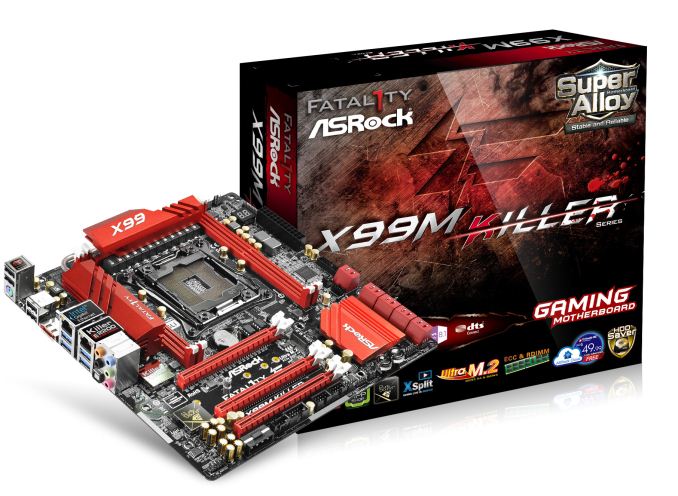

Due to the size, if any other mATX motherboards are released I would assume that like the X99M Killer there will only be four DDR4 memory slots, and here ASRock have used thinner slots in order to fit the power delivery and other features on board. I count five fan headers on the board, along with ASRock’s HDD Saver connector and ten SATA 6 Gbps ports. I can just about make out that some of these are labelled SATA3_0_1 and some are labelled 5_SATA3_0_1, perhaps indicating the presence of a controller or a hub. There is also a USB 3.0 header on board with power/reset buttons, a two digit debug, two BIOS chips, two USB 2.0 headers, a COM header and additional power to the PCIe slots via s 4-pin molex. We also have an eSATA on the rear panel, with a ClearCMOS button.

The box lists XSplit, indicating a bundling deal with the software, as well as ECC and RDIMM support. I believe the X99M Killer will be due out at launch, or relatively soon after, although ASRock has not released the pricing details yet.
Read More ...
Intel Demonstrates Direct3D 12 Performance and Power Improvements
However at the opposite end of the spectrum and away from the performance benefits are the efficiency benefits, and those are gains that haven’t been covered nearly as well. With that subject in mind, Intel is doing just that this week at SIGGRAPH 2014, where the company is showcasing both the performance and efficiency gains from Direct3D 12 on their hardware.
When it comes to power efficiency Intel stands to be among the biggest beneficiaries of Direct3D 12 due to the fact that they exclusvely ship their GPUs as part of an integrated CPU/GPU product. Because the GPU and CPU portions of their chips share a thermal and power budget, by reducing the software/CPU overhead of Direct3D, Intel can offer both improved performance and power usage with the exact same silicon in the same thermal environment. With Intel's recent focus on power consumption, mobile form factors, and chips like Core M, Direct3D 12 is an obvious boon to Intel.
Intel wisely demonstrated this improvement using a modern low-power mobile device: the Microsoft Surface Pro 3. For this demo Intel is using the Core i5-4300U version, Microsoft’s middle of the road model that clocks up to 2.9GHz on the CPU and features one of Intel’s HD 4400 GPUs, with a maximum GPU clockspeed of 1.1GHz. In our testing, we found the Surface Pro 3 to be thermally constrained – throttling when met with a medium to long duration GPU task. Broadwell should go a long way to improve the situation, and so should Direct3D 12 for current and future Intel devices.
To demonstrate the benefits of Direct3D 12, Intel put together a tech demo that renders 50,000 unique asteroid objects floating in space. The demo can operate in maximum performance mode with the frame rate unrestricted, as well as a fixed frame rate mode to limit CPU and GPU utilization in order to reduce power consumption. The demo can also dynamically switch between making Direct3D 11 and Direct3D 12 API calls. Additionally, an overlay shows power consumption of both the CPU and GPU portions of the Intel processor.
Intel states this demo data was taken after steady-state thermals were reached.


To put these numbers in perspective, a 50% reduction in power consumption is about what we would see from a new silicon process (i.e. moving from 22nm to 14nm), so to achieve such a reduction in consumption with software alone is a very significant result and a feather in Microsoft’s cap for Direct3D 12. If this carries over to when DirectX 12 games and applications launch in Q4 2015, it could help usher in a new era of mobile gaming and high end graphics. It is not often we see such a substantial power and performance improvement from a software update.
Source: Intel, Microsoft
Read More ...
Corsair Carbide Air 240 Case Review
With compact cases and SSFs being all the rage nowadays, today Corsair is launching the Carbide Air 240, a cubic Micro-ATX case designed to fit powerful PC hardware. As the name suggests, it is based on the design of the Full-ATX Carbide Air 540 that released last year. Can the smaller version make the same impact impact as its larger, older brother? We will find out in this review.
Read More ...
Isolated Internet Outages Caused By BGP Spike

Two days later, and there is a pretty clear understanding of what happened. Older Cisco core internet routers with a default configuration only allowed for a maximum 512k routes for their Border Gateway Protocol (BGP) tables. With the internet always growing, the number of routes surpassed that number briefly on Tuesday, which caused many core routers to be unable to route traffic.
BGP is not something that is discussed very much, due to the average person never needing to worry about it, but it is one of the most used and most important protocols on the internet. The worst part of the outage was that it was known well in advance that this would be an issue, yet it still happened.
Let us dig into the root cause. Most of us have a home network of some sort, with a router, and maybe a dozen or so devices on the network. We connect to an internet service provider through (generally) a modem. When devices on your local network want to talk to other devices on your network, they do so by sending packets upstream to the switch (which is in most cases part of the router) and then the switch forwards the packet to the correct port where the other device is connected. If the second device is not on the local network, the packets get sent to the default gateway which then forwards them upstream to the ISP. At the ISP level, in simple terms, it works very similarly to your LAN. The packet comes in to the ISP network, and if the IP address is something that is in the ISP’s network, it gets routed there, but if it is something on the internet, the packet is forwarded. The big difference though is that an ISP does not have a single default gateway, but instead connects to several internet backbones. The method in which internet packages are routed is based on the Border Gateway Protocol. The BGP contains a table of IP subnets, and lists which ports to transfer traffic based on rules and paths laid out by the network administrator. For instance, if you want to connect to Google to check your Gmail, your computer will send a TCP connection to 173.194.33.111 (or another address as determined by your DNS settings and location). Your ISP will receive this packet, and send the packet to the correct port to an outbound part of the internet which is closer to the subnet that the address is in. If you then want to connect to Anandtech.com, the packet will be sent to 192.65.241.100, and the BGP protocol of the ISP router will then send to possibly a different port. This continues upstream from core router to core router until the packet reaches the destination subnet, where it is then sent to the web server.

The actual specifics of what happened seemed to be that Verizon unintentionally added approximately 15,000 /24 routes into the global routing table. These prefixes were supposed to be aggregated, but this didn’t happen, and as such, the total number of subnet prefixes in the table spiked. Verizon fixed the mistake quickly, but it still caused many routers to fail.
Although you could be quick to jump and blame Verizon for the outage, it has to be noted that Cisco issued a warning to customers explaining that the memory which is allocated for the BGP table would be very close to being full, and gave specific instructions on how to correct it. This warning came several months ago. Unfortunately not all customers of Cisco heeded or received the warning, which caused the brief spike to cripple parts of the internet.
Newer Cisco routers were not affected, because the default configuration for the TCAM memory which is designated for the BGP table allows for more than 512,000 entries. Older routers from Cisco have enough physical memory for up to 1,000,000 entries, assuming the configuration was changed as outlined by Cisco.
The effects of outages like this can be quite potent on the internet economy, with several online services being unavailable for large parts of the day. However this outage doesn’t need to happen again, even though the steady state number of entries in the BGP table will likely exceed magic 512,000 number again. Hopefully with this brief outage, lessons can be learned, and equipment can be re-configured or upgraded which will prevent this particular issue from rearing its head again in the future.
Sources
DSLReports
Renesys
BGPMon
Read More ...
HTC Launches Zoe Beta: Hands On and First Impressions


As of publication, the HTC Zoe Beta is available on the Play Store. HTC has stated that Android 4.4 devices should be compatible with this application although there may be additional restrictions.
Read More ...
be quiet! Power Zone 850W CM Power Supply Review
be quiet! is a German company that specializes in low-noise computer PSUs and coolers, and they are slowly making their way into the North American market. Today we have their Power Zone 850W CM in our labs for review, an apparently popular but expensive power supply. Read on to see if it warrants the high price.
Read More ...
ASUS ROG Z97 Maximus VII Impact Officially Launched
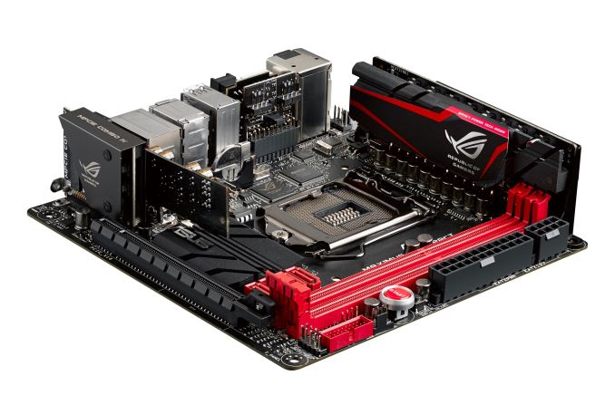
Similar to the Maximus VI, the order of the day is extra PCBs in order to add features. The power delivery is upgraded to the ROG 9-series design, and the audio add-on SupremeFX card moves up with fewer filter caps in a more optimized output. The mPCIe Combo moves up to revision four which includes a PCIe 3.0 x4 M.2 slot and a mini-PCIe slot with a bundled 802.11ac dual band WiFi module. Note that when the M.2 slot is occupied, the PCIe slot will reduce to PCIe 3.0 x8, although our previous testing of a similar feature shows no frame rate difference at 1080p.

Interestingly enough the rear of the Impact Control is another PCB, holding two 4-pin fan headers to compliment the 4-pin CPU fan header on the top left and the chassis header on the right of the motherboard. Also of note is the rear panel, where a single block of USB ports uses two USB 3.0 ports and two USB 2.0 ports – this configuration I have not seen on a motherboard before and could pave the way for something on most motherboards for the future.

The socket area is up against Intel specifications, suggesting that CPU coolers might be up against the power delivery or tall memory modules. The audio is buffeted by Sonic Rader II, an onscreen representation of directional audio, and networking comes via the 802.11ac WiFi and an Intel I218-V with GameFirst III.

Read More ...
Comcast, TWC Pull Dinner Gift for FCC Commissioner... Sort Of
Both companies cited criticism, claim public "misunderstood" their efforts
Read More ...
Report: Windows 9 “Threshold” Tech Preview Coming Next Month
According to Mary Jo Foley, the tech preview will be open to the public and will be available in late September
Read More ...
Windows Phone, BlackBerry Smartphone Market Share Falls to 2.5%, 0.5% Respectively
The latest figures from IDC show that Microsoft and BlackBerry have a lot of work to to do to reclaim lost market share
Read More ...
Smarter Wired, Wireless Chargers Set to Shake Up Mobile Industry
Charger heal thyself
Read More ...
Cell Phone Thief Calls 911 After Her Victim Chases Her and Her Male Cohort
Boyfriend/co-conspirator abandoned suspect and ran off; cops find a modest size crack rock on the female suspect
Read More ...
Ford Partners with DTE Energy to Deploy MI’s Largest Solar Installation
New solar array will have the capacity to charge thirty electric or plug-in hybrid vehicles
Read More ...
Update: Samsung Gets Official With 4.7”, Aluminum-frame Galaxy Alpha Smartphone
Samsung prepares to take on the existing iPhone 5S and the upcoming 4.7" iPhone 6
Read More ...
Beastly Samsung Galaxy Note 4 Specs Revealed: Snapdragon 805 Processor, 4GB RAM
Galaxy Note 4 will also include a 16MP rear camera with OIS
Read More ...
Available Tags:GIGABYTE , ASUS , ASRock , Intel , HTC , Windows , Market Share , Windows Phone , BlackBerry , Smartphone , Wireless , Ford , Samsung , Galaxy ,
No comments:
Post a Comment