
The HTC One (M8) Review
HTC remains one of few Android OEMs insanely focused on design. Even dating back to the origins of the One brand in 2012 with the One X and One S, HTC clearly saw design where others were more focused on cost optimization. Only time will tell which is the more viable long term business strategy, but in the interim we’ve seen two generations of well crafted devices from what would otherwise be thought of as a highly unlikely source. With its roots in the ODM/OEM space, HTC is one of very few ODM turned retail success stories that we’ve seen come out of Taiwan. ASUS is the closest and only real comparison I can make.
As its name implies, the goal of the One brand was to have a device that anyone, anywhere in the world could ask for and know they were getting an excellent experience. Although HTC sort of flubbed the original intent by introducing multiple derivatives (One X, One S, One X+), it was the beginning of relief from the sort of Android OEM spaghetti we saw not too long ago. With the One brand, HTC brought focus to its product line.
Last year HTC took a significant step towards evolving the brand into one true flagship device, aptly named the One. Once again there were derivatives (One mini and One max), but the messaging was far less confusing this time around. If you wanted small you got the mini, if you wanted big you got the max, otherwise all you needed to ask for was the One.
With last year’s One (codenamed M7), HTC was incredibly ambitious. Embracing a nearly all metal design and opting for a much lower resolution, but larger format rear camera sensor, the One was not only bold but quite costly to make. With the premium smartphone market dominated by Apple and Samsung, and the rest of the world headed to lower cost devices, it was a risky proposition. From a product standpoint, I’d consider the M7 One a success. A year ago I found myself calling it the best Android phone I’d ever used.
It didn’t take long for my obsession to shift to the Moto X, and then the Nexus 5, although neither delivered the overall camera experience of the One. Neither device came close to equaling HTC on the design front either, although I maintain Motorola did a great job with in hand feel. Although I found myself moving to newer devices since my time with the One last year, anytime I picked up the old M7 I was quickly reminded that HTC built a device unlike any other in the Android space. It just needed a refresh.
This is our review of the new HTC One.
Read More ...
AMD Announces FirePro W9100
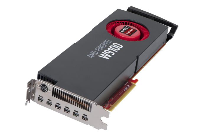
As Hawaii itself was a small but important refresh to Tahiti and the GCN architecture, the same can be said of the FirePro W9100 compared to the FirePro W9000. Other than some gaming-exclusive features such as TrueAudio, Hawaii’s biggest changes were the Asynchronous Compute Engine (ACE) additions that are part of GCN 1.1, the wider 4 primitive geometry pipeline, and of course the overall increase in performance and performance per watt compared to Tahiti. So from a technical perspective W9100 stands to be a relatively straightforward improvement to what W9000 has offered thus far.
AMD FirePro W Series Specification Comparison |
||||||
AMD FirePro W9100 |
AMD FirePro W9000 |
AMD FirePro W8000 |
AMD FirePro W7000 |
|||
Stream Processors |
2816 |
2048 |
1792 |
1280 |
||
Texture Units |
176 |
128 |
112 |
80 |
||
ROPs |
? |
32 |
32 |
32 |
||
Core Clock |
? |
975MHz |
900MHz |
950MHz |
||
Memory Clock |
? |
5.5GHz GDDR5 |
5.5GHz GDDR5 |
4.8GHz GDDR5 |
||
Memory Bus Width |
? |
384-bit |
256-bit |
256-bit |
||
VRAM |
16GB |
6GB |
4GB |
4GB |
||
Double Precision |
1/2? |
1/4 |
1/4 |
1/16 |
||
Transistor Count |
6.2B |
4.31B |
4.31B |
2.8B |
||
TDP |
? |
274W |
189W |
<150W |
||
Manufacturing Process |
TSMC 28nm |
TSMC 28nm |
TSMC 28nm |
TSMC 28nm |
||
Architecture |
GCN 1.1 |
GCN 1.0 |
GCN 1.0 |
GCN 1.0 |
||
Warranty |
3-Year |
3-Year |
3-Year |
3-Year |
||
Launch Price |
? |
$3999 |
$1599 |
$899 |
||
Speaking of the memory bus, we don’t have the specific width or clockspeeds there either, but we know that AMD has packed W9100 with a ton of memory. 16GB of memory to be precise, which would be as much memory as Hawaii would be able to handle using current generation 8Gb GDDR5 modules. Compared to even W9000, which was relatively large for its time at 6GB, this is huge for a workstation card.

Beyond that, we don’t have any further details on the card at this time. W9100 is not launching today – we hear the launch should be soon after – so availability and pricing have not been released thus far. The best we can do is point to the W9000’s launch price of $3999 as some kind of guidance on where it may come in.
Shifting gears for a bit, while AMD was careful on releasing details ahead of the launch of the W9100, they spent some time going in depth into how the card fits into their long-term plans, and what markets they’re pursuing with the card. FirePro continues to pull double duty as AMD’s workstation graphics card and workstation compute card, centered around the capabilities of OpenCL. So AMD is looking to put together a product that can serve both markets well, especially in the case of cross-over applications that make use of both aspects of the card.


Finally, the launch of the W9100 also brings with it a brief update on AMD’s overall transformation in their product offerings, and their current market share. AMD’s share of the professional GPU market is up to 18%, which is still well off of their heyday years ago, but a solid improvement from where they were at the launch of the W9000. To that end professional graphics and compute continues to represent a major growth opportunity for the company, as the other 82% of that market share belongs to NVIDIA, and stealing even a small part of it would significantly improve AMD’s position. Next to their APU offerings – including semi-custom designs and ARM designs – the discrete GPU market for professional graphics is AMD’s final target for significant growth.


Read More ...
Asustor AS-304T: 4-Bay Intel Evansport NAS Review
Intel's Evansport NAS platform was meant to take on ARM's dominance in the low to mid-range consumer / SOHO NAS market. We covered it in detail while reviewing the Thecus N2560, a 2-bay solution. How does the platform fare in a unit with four bays? Read on for our report from the evaluation of Asustor's AS-304T to find out.
Read More ...
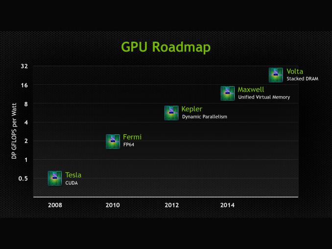
NVIDIA Updates GPU Roadmap; Unveils Pascal Architecture For 2016

We’ll get to Pascal in a second, but to put it into context let’s first discuss NVIDIA’s restructuring. At GTC 2013 NVIDIA announced their future Volta architecture. Volta, which had no scheduled date at the time, would be the GPU after Maxwell. Volta’s marquee feature would be on-package DRAM, utilizing Through Silicon Vias (TSVs) to die stack memory and place it on the same package as the GPU. Meanwhile in that roadmap NVIDIA also gave Maxwell a date and a marquee feature: 2014, and Unified Virtual Memory.
NVIDIA's Old Volta Roadmap

NVIDIA's New Pascal Roadmap
As far as NVIDIA is concerned, Maxwell’s marquee feature is now DirectX 12 support (though even the extent of this isn’t perfectly clear), and that with the shipment of the GeForce GTX 750 series, Maxwell is now shipping in 2014 as scheduled. We’re still expecting second generation Maxwell products, but at this juncture it does not look like we should be expecting any additional functionality beyond what Big Kepler + 1st Gen Maxwell can achieve.
Meanwhile Volta has been pushed back and stripped of its marquee feature. It’s on-package DRAM has been promoted to the GPU before Volta, and while Volta still exists, publicly it is a blank slate. We do not know anything else about Volta beyond the fact that it will come after the 2016 GPU.
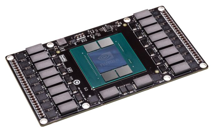
Which brings us to Pascal, the 2016 GPU. Pascal is NVIDIA’s latest GPU architecture and is being introduced in between Maxwell and Volta. In the process it has absorbed old Maxwell’s unified virtual memory support and old Volta’s on-package DRAM, integrating those feature additions into a single new product.

Meanwhile NVIDIA hasn’t said anything else directly about the unified memory plans that Pascal has inherited from old Maxwell. However after we get to the final pillar of Pascal, how that will fit in should make more sense.

The end result is a bus that looks a whole heck of a lot like PCIe, and is even programmed like PCIe, but operates with tighter requirements and a true point-to-point design. NVLink uses differential signaling (like PCIe), with the smallest unit of connectivity being a “block.” A block contains 8 lanes, each rated for 20Gbps, for a combined bandwidth of 20GB/sec. In terms of transfers per second this puts NVLink at roughly 20 gigatransfers/second, as compared to an already staggering 8GT/sec for PCIe 3.0, indicating at just how high a frequency this bus is planned to run at.

But the rabbit hole goes deeper. To pull off the kind of transfer rates NVIDIA wants to accomplish, the traditional PCI/PCIe style edge connector is no good; if nothing else the lengths that can be supported by such a fast bus are too short. So NVLink will be ditching the slot in favor of what NVIDIA is labeling a mezzanine connector, the type of connector typically used to sandwich multiple PCBs together (think GTX 295). We haven’t seen the connector yet, but it goes without saying that this requires a major change in motherboard designs for the boards that will support NVLink. The upside of this however is that with this change and the use of a true point-to-point bus, what NVIDIA is proposing is for all practical purposes a socketed GPU, just with the memory and power delivery circuitry on the GPU instead of on the motherboard.

Molex's NeoScale: An example of a modern, high bandwidth mezzanine connector
With all of that said, while NVIDIA has grand plans for NVLink, it’s also clear that PCIe isn’t going to be completely replaced anytime soon on a large scale. NVIDIA will still support PCIe – in fact the blocks can talk PCIe or NVLink – and even in NVLink setups there are certain command and control communiques that must be sent through PCIe rather than NVLink. In other words, PCIe will still be supported across NVIDIA's product lines, with NVLink existing as a high performance alternative for the appropriate product lines. The best case scenario for NVLink right now is that it takes hold in servers, while workstations and consumers would continue to use PCIe as they do today.

Finally, NVIDIA has already worked out some feature goals for what they want to do with NVLink 2.0, which would come on the GPU after Pascal (which by NV’s other statements should be Volta). NVLink 2.0 would introduce cache coherency to the interface and processors on it, which would allow for further performance improvements and the ability to more readily execute programs in a heterogeneous manner, as cache coherency is a precursor to tightly shared memory.
Wrapping things up, with an attached date for Pascal and numerous features now billed for that product, NVIDIA looks to have to set the wheels in motion for developing the GPU they’d like to have in 2016. The roadmap alteration we’ve seen today is unexpected to say the least, but Pascal is on much more solid footing than old Volta was in 2013. In the meantime we’re still waiting to see what Maxwell will bring NVIDIA’s professional products, and it looks like we’ll be waiting a bit longer to get the answer to that question.
Read More ...
Spotify Introduces $4.99 Premium Subscription for College Students in the US
Spotify
is already one of the most popular music streaming services on the
planet with over 24 million active users, and over a fourth of them (~ 6
million) being Spotify Premium subscribers. Spotify was in the news
back in January when it introduced ad-supported, no-limits streaming on
the desktop and across iOS and Android devices, just in time for the
launch of the Beats Music streaming service.
Today's
announcement is squarely targeted towards the college demographic in the
US, which can now avail an ad-free, unlimited streaming, Spotify
Premium subscription for $4.99 a month as long as they provide proof of
their current enrollment status at a valid educational institute in the
United States. The offer works with both new and existing accounts, and
current Premium subscribers can transition to the discounted plan at the
end of their current billing cycle. So long as as their student
admission status is maintained, the offer can be extended up to a
maximum of three times.I have personally been a huge fan of Spotify and a Premium subscriber for over 2 years now, and would have jumped at such an opportunity, had it presented itself while I was still in college. Those amongst us still lucky to be in college can follow the link below for instant gratification.
Source: Spotify, Terms & Conditions
Read More ...
Android has 97 Percent of Mobile Malware, But Nearly None in the U.S.
But almost all of that comes from third party apps stores in Asia and the Middle East
Read More ...
World Trade Org. to China on Rare Earth Metals: Stop Breaking the Law
... or else we'll do something really bad to you (except that we can't)
Read More ...
New Encryption System "Mylar" Encrypts Data in Browser Before Reaching Server
This will stop websites from leaking data
Read More ...
BlackBerry Executive Ordered to Fulfill 6-Month Resignation Term Before Leaving for Apple
He tried to leave ahead of time despite his contract
Read More ...
F-35 Lightning II Chosen by South Korea as More Software Delays Loom
F-35 program gets some good news and some bad news
Read More ...
Sprint CEO Dan Hesse Tips Nationwide HD Voice Rollout for July
"Voice is still the killer app" -- Sprint CEO Dan Hesse
Read More ...
Volvo "Flybrid" KERS System Promises to Reduce Fuel Consumption by 25%
Volvo testing a prototype of the KERS system right now
Read More ...
Available Tags:HTC , AMD , FirePro , Intel , NVIDIA , GPU , Android , Server , BlackBerry , Apple , CEO , Volvo ,
No comments:
Post a Comment