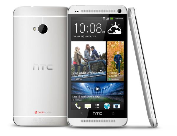
 Hands on and Impressions from the HTC One - Formerly M7
HTC is in an interesting position as a result of this last product cycle. While the previous HTC One series’ industrial design and performance was top notch, other OEMs still managed to eclipse the One series in terms of market adoption and consumer perception. Getting back to being a solid performer and cementing a place as at least the dominant number three player in the smartphone space is HTC’s mission for 2013, and the flagship device it’s starting that out with is the device previously known as M7, now known simply as the HTC One.
Read on for our analysis of the new HTC One!


 Read More ...
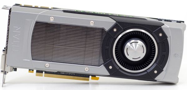
NVIDIA's GeForce GTX Titan, Part 1: Titan For Gaming, Titan For Compute
Last year's launch of the Titan supercomputer was a major win for NVIDIA, and likely the breakthrough they’ve been looking for. A fledging business merely two generations prior, NVIDIA and their Tesla family have quickly shot up in prestige and size, much to the delight of NVIDIA. Their GPU computing business is still relatively small, but it’s now a proven business for NVIDIA. More to the point however, winning contracts like Titan are a major source of press and goodwill for the company, and goodwill the company intends to capitalize on.
With the launch of the Titan supercomputer and the Tesla K20 family now behind them, NVIDIA is now ready to focus their attention back on the consumer market. Ready to bring their big and powerful GK110 GPU to the consumer market, in typical NVIDIA fashion they intend to make a spectacle of it. In NVIDIA’s mind there’s only one name suitable for the first consumer card born of the same GPU as their greatest computing project: GeForce GTX Titan.


 Read More ...
High-End Meets Small Form Factor: GeForce Titan in Falcon Northwest's Tiki
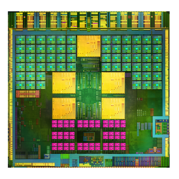
Today NVIDIA officially unveiled its first consumer facing GK110 graphics card: the GeForce Titan. Although
GK110 launched last year, gamers didn't have access to it as it launched exclusively as a Tesla part. No less than 18,688 GK110 based Tesla K20X GPUs were deployed in the
Titan Supercomputer at the Oak Ridge National Laboratory, which did a good job of eating up almost all GK110 production. With the Titan Supercomputer launched and out of the way, GK110 could make its way into the consumer space. The development costs and effort to bring a 7.1 billion transistor chip to market are huge, so it makes sense to try and sell as many chips as possible, even if they're well above the sweet spot on the price/performance curve.
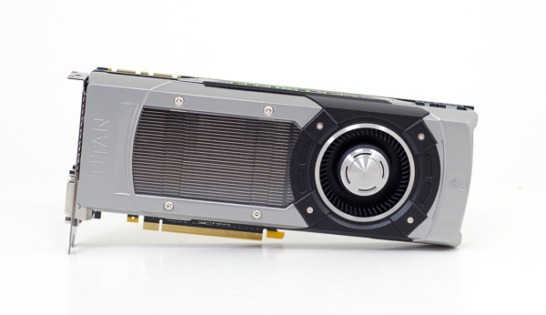
NVIDIA saw three target markets for GeForce Titan: 1) CUDA developers, 2) ultra high-end gamers looking for great 3-way SLI performance and 3) users looking to build a high-end small form factor gaming machine that only has room for a single, dual-slot graphics card at most. The first group is easy to address, and later this week we'll have compute benchmarks to begin to address that community (and perhaps even more over the coming months). It's the second and third groups that require a somewhat different approach.
To showcase what could be done with GeForce Titan, NVIDIA asked some of its closest system builder partners to build gaming systems around the new GPU. We had the choice of getting either a 3-way SLI system or a single card, small form factor machine.
This is our experience with Titan in one of the most exciting small form factor systems on the market today: Falcon Northwest's Tiki. Read on!
 Read More ...
NVIDIA Announces Tegra 4i, Formerly Project Grey, With Integrated LTE and Phoenix Reference Design
It has been a while since we’ve heard anything about Project Grey, the first NVIDIA SoC with an integrated digital baseband, and the result of NVIDIA’s acquisition of soft-modem manufacturer Icera. Today, NVIDIA is ready to formalize Project Grey as Tegra 4i, and we have a bunch of information about this SoC and will obtain even more before MWC is upon us. NVIDIA’s
roadmap from late 2011 put Grey in early 2013, and while other members of that roadmap haven’t necessarily stuck to the promised release schedule, Grey seems to be somewhere close to that schedule, at least as far as announcement and samples are concerned.
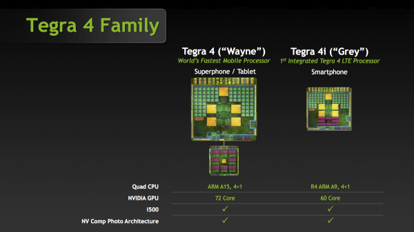
First, Tegra 4i includes the familiar 4+1 arrangement of cores we've seen since Tegra 3, but instead of Tegra 4's A15s, 4i includes ARM Cortex A9 CPUs running at a maximum single core clock of 2.3 GHz, we’re still waiting on a breakdown of the clock rates for dual and quad configuration, as well as the shadow core. NVIDIA has noted that it using R4 of ARM’s Cortex A9, which includes higher IPC thanks to the addition of a better data prefetching engine, dedicated hardware for cache preload instructions and some larger buffers. NVIDIA believes it is the first to implement the latest version of ARM's Cortex A9 core, however there's nothing stopping others from doing the same.
NVIDIA likely chose to integrate ARM's Cortex A9 r4 instead of the Cortex A15 to reduce power consumption and die size. While Tegra 4 is expected to be around 80mm^2, Tegra 4i measures in at around 60mm^2 including integrated baseband. NVIDIA isn't talking about memory interfaces at this point, but do keep in mind that your memory interface is often defined by the size of your die.

The 4i SoC is also built on TSMC’s 28 HPM process, interestingly enough not the 28 HPL process used for Tegra 4. As Tegra 4i appears to be geared towards hitting very high clock speeds, the use of TSMC's 28nm HPM process makes sense.
Tegra 4i also gets the exact same ISP and computational photography features that Tegra 4 includes, along with the same video encode and decode blocks. When it comes to the GPU side, 4i includes 60 GPU cores, that's just shy of the 72 in Tegra 4 proper. We’re waiting on additional detail to understand if these cores include the
same enhancements we saw in Tegra 4 vs. Tegra 3. We also don't know the clock speed of the GPU cores in Tegra 4i.
| Tegra 4 Comparison |
| Tegra 4 | Tegra 4i |
| CPU Configuration | 4+1 ARM Cortex A15 | 4+1 ARM Cortex A9 "r4" |
| Single CPU Max Clock | 1.9 GHz | 2.3 GHz |
| Process | 28nm HPL | 28nm HPM |
| GPU Cores | 72 | 60 |
| Memory Interface | PCDDR3 and LPDDR3 | LPDDR3 |
| Display | 3200x2000 | 1920x1200 |
| Baseband | No Integrated Modem | Icera i500
LTE Cat 3/Cat 4+CA TDD,FDD
100-150 Mbps DL (50 Mbps UL)
TMs 1-8
WCDMA Cat 24/6 42 Mbps
DL (5.7 Mbps UL)Cat 24/6
TD-HSPA 4.2 Mbps DL
(2.2 Mbps UL) Including TD-SCDMA |
| Package | 23x23 BGA
14x14 FCCSP | 12x12 POP
12x12 FCCSP |
Tegra 4i also includes the Icera i500 baseband IP block on-die, hence i for Icera. NVIDIA has disclosed some additional detail about i500 along the lines of what we’ve already written about. There’s full support for Category 3 (100 Mbps) LTE at launch, with a later upgrade to Category 4, along with support for 10 MHz + 10 MHz LTE carrier aggregation. In addition there’s support for the rest of the 3GPP suite of air interfaces, including WCDMA / HSPA+ up to 42 Mbps (Category 24), TD-SCDMA, and GSM/EDGE. i500 is also voice enabled with VoLTE support and CS-FB voice modes. NVIDIA claims that the i500 package is 7x7mm with a 6.5x6.5mm transceiver, and there are a total of 8 primary Rx ports (bands). NVIDIA also claims support for both 2x2 MIMO and 4x4 MIMO transmission modes on LTE.
Functionally Tegra 4i is more like a heavily upgraded Tegra 3 than a Tegra 4 part thanks to the Cortex A9s. It's clear that Tegra 4i is aimed more at the smartphone market while Tegra 4 proper aims at tablets or other platforms with a higher power budget and greater performance demands.
In terms of time frame, NVIDIA expects the first Tegra 4i designs to begin shipping at the end of 2013, with most devices appearing in Q1 of 2014. It'll be interesting to see how a Cortex A9 based design holds up in Q1 2014, although the newer core and very high clock speed should do a good job of keeping the SoC feeling more modern than you'd otherwise expect.

The other big announcement is a reference design built around Tegra 4i called Phoenix. It's a smartphone with Tegra 4i inside, 5-inch 1080p display, LTE, and just 8 mm of thickness. What's more impressive is that NVIDIA claims the reference design can be picked up by an OEM and ship with an unsubsidized price tag of between $100-$300 USD. With Phoenix NVIDIA now joins the likes of Qualcomm and Intel, both of whom already have active smartphone reference design programs.
We have a lot more questions about Tegra 4, 4i, and Phoenix, but answers are coming.


 Read More ...
HTC NYC Event: Live Blog
Join us right here at 10AM EST today as we live blog HTC's big NYC event. We'll hopefully find out what HTC's got under wraps. Afterwards stay tuned for our hands-on and more details as we get them.

mage courtesy of HTCGlobal on Instagram


 Read More ...
Available Tags:
HTC ,
GeForce ,
GTX ,
NVIDIA ,


No comments:
Post a Comment