
Microsoft to Recall Power Cables for Previous-Gen Surface Pro Tablets
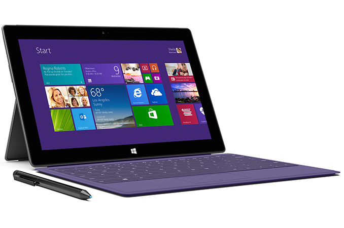
Power cables of Surface Pro, Surface Pro 2 and Surface Pro 3 are vulnerable to overheating and could pose a fire hazard after they are sharply or repeatedly bent or tightly wrapped, according to Microsoft. Microsoft did not name the supplier of the power cords it shipped for about three years. The potentially dangerous cables look like regular power cords used with variety of notebook PSUs. Such cables are not very bendable and, as it appears, can be damaged. Fortunately, they are detachable and users, who want to replace their cables now, can do so without waiting for Microsoft.
On Wednesday the company confirmed to ZDNet that the recall will be taking place, and will officially issue a statement on the matter of Surface Pro power cables early on Friday. The voluntary recall will be applied to all devices sold before mid-July, 2015, worldwide. Eligible customers wishing to get a replacement will have to order it via a special web-site. Microsoft plans to advice customers to stop using potentially dangerous power cords and to dispose of them in accordance with local regulations.
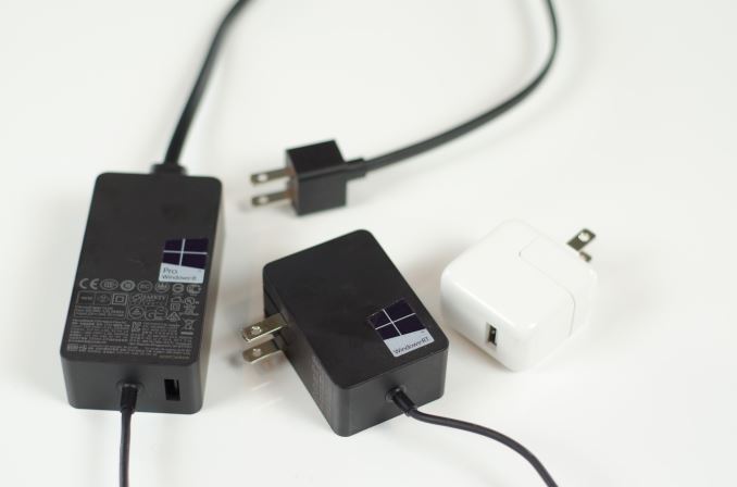
Microsoft Surface Pro charger is on the left side of the picture.
Microsoft’s Surface (non-Pro) slates as well as the latest Surface Pro 4 tablets are not affected, the software giant said, reports Channelnomics.eu.
The first-generation Surface Pro was introduced along with the Windows 8 operating system in October, 2012. It became available in early 2013 and was replaced by the Surface Pro 2 later that year. The third-generation Surface Pro hit the market in mid-2014. To date, Microsoft has sold millions of its slates, which it positions as notebook replacement tablets.
Many power cords should not be bent or wrapped too tightly because they can be damaged this way. Some companies try to use softer cables and/or equip their cables with some form of cable management. Unfortunately, power cords of Microsoft Surface Pro only come with a tiny hook.
Keeping in mind that so far, there have been no reports about overheating cables or PSUs of Microsoft’s Surface Pro tablets, the cables should be generally safe to use. Nonetheless, it is somewhat sad that Microsoft has not discovered the potential issue earlier.
Read More ...
Securifi Updates Smart Home Hub Lineup with New Almond 3 Wireless Router
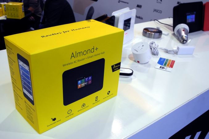
Securifi's family of routers (the Almonds) consists of two product lines - one targeting the high-end market and the other aiming to be more affordable. At CES, Securifi launched the Almond 3, a new member in the second category. The following extract from the press brochure shows how the currently available models compare against each other.
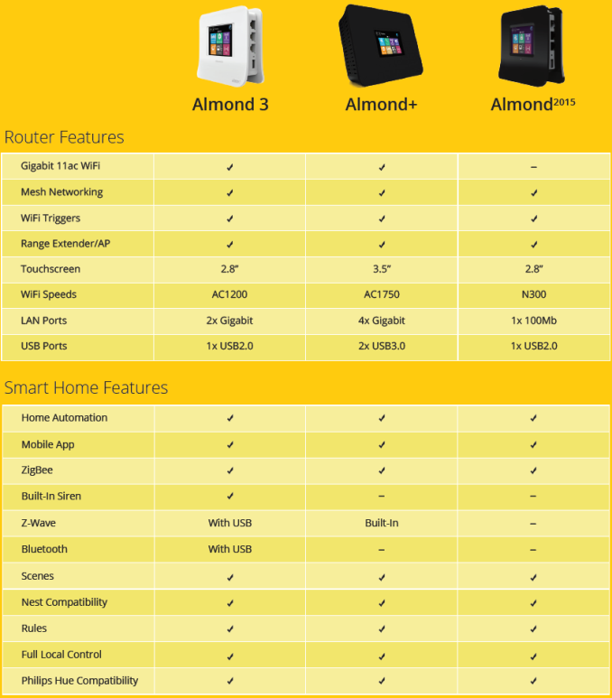
It is obvious that the Almond+ belongs to the high-end line, while the Almond 3 belongs to the affordable category. Like the Almond 2015, the Almond 3 is also based on a Mediatek chipset. The chipset used is likely to be the MT7612E along with MT7621N SoC (waiting for confirmation from Securifi for this). It is an AC1200 router (2x2 802.11ac for 867 MBps in the 5 GHz band and 2x2 in the 2.4 GHz band for 300 Mbps).
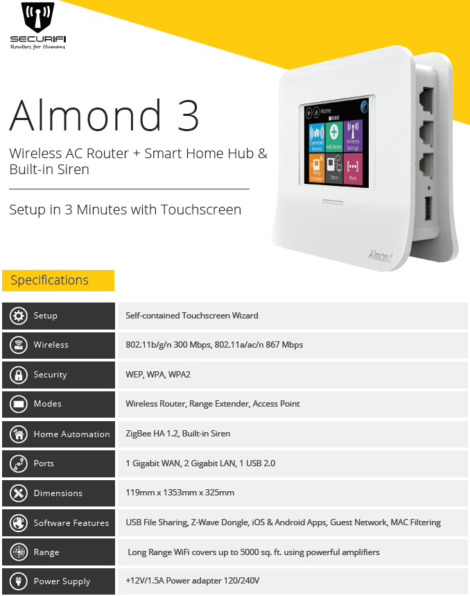
The above specifications indicate that the Almond 3 is a definite step up from the Almond 2015, which was a 100 Mbps N300 router. The built-in siren enables some interesting scenarios, particularly as a security alarm when combined with ZigBee door / window magnetic reed sensors. Considering the specifications and the focus on user experience with the touchscreen interface, the Almond 3 targets the average consumer.
Integrating home automation radios in the hardware for the router is only one side of the equation. Other vendors (like Google via TP-Link and Asus and TP-Link itself) have also started to explore this area. The other important ingredient for market success is the user experience. Perfecting the web user interface as well as the mobile apps is a challenge, particularly when home automation is involved.
At CES, Securifi demonstrated their mobile app, and I have to say that it has one of the most user-friendly interfaces to setting up the 'rules and scenes' (i.e, how changes reported by one sensor (or, even just the time) can be used to trigger events in other connected devices). They also talked about an innovative idea for implementing geofencing by recognizing the connection status of the user's smartphone in the router.
Securifi has also opened up their Websockets API. This should help power users and third-party developers to interface with the Almonds / home automation devices and develop their own applications. The other important takeaway from my conversation with Securifi was that they have implemented full cloud-less control of all supported home automation devices on all the Almond routers. I have always been a big proponent of isolating home automation devices from the Internet for security and reliability purposes. Power users on the go have multiple ways to obtain access to the home automation controller (in this case, the Almond device) over the Internet - including, but not restricted to, running a VPN server in the home network. On a general note, I am waiting for a consumer networking equipment vendor to make VPNs more accessible to the general audience. This will be very useful for consumers who don't want their home automation devices to be at the mercy of a cloud server somewhere on the Internet.
The Almond 3 is slated to become available later this quarter. It will retail for $119. Coupled with a sensor such as this, we believe it is a value-focused solution for the average consumer's networking and security alarm needs.
Read More ...
JEDEC Publishes HBM2 Specification as Samsung Begins Mass Production of Chips
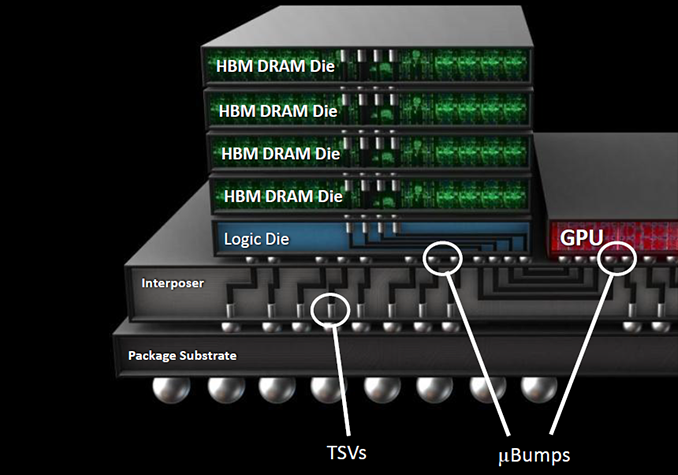
JEDEC, a major semiconductor engineering trade organization that sets standards for DRAM, recently published the final specifications of the second-generation HBM (HBM2), which means that members of the organization had ratified the standard. The new memory technology builds upon the foundation of the original JESD235 standard, which describes stacked memory devices interconnected using through silicon vias (TSVs) with a very wide input/output (I/O) interface operating at moderate data-rates. The JESD235A will help engineers to further increase performance, capacity and capabilities of HBM memory chips. HBM Gen 2 will be particularly useful for the upcoming video cards by AMD and NVIDIA, which thanks to HBM2 can feature as much as 512 GB/s – 1 TB/s of memory bandwidth and 8, 16 or even 32 GB of memory onboard.
HBM Gen 1: Good, But With Limitations
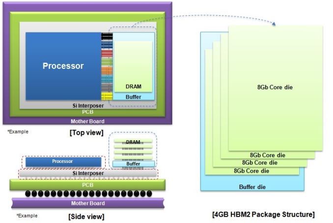
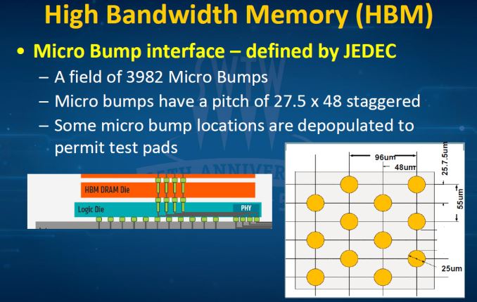
The original JESD235 standard defines the first-generation HBM (HBM1) memory chips with a 1024-bit interface and up to 1 Gb/s data-rate, which stack two, four or eight DRAM devices with two 128-bit channels per device on a base logic die. Each HBM stack (which is also called KGSD — known good stacked die) supports up to eight 128-bit channels because its physical interface is limited to 1024 bits. Every channel is essentially a 128-bit DDR interface with 2n prefetch architecture (256 bits per memory read and write access) that has its own DRAM banks (8 or 16 banks, depending on density), command and data interface, clock-rate, timings, etc. Each channel can work independently from other channels in the stack or even within one DRAM die. HBM stacks use passive silicon interposers to connect to host processors (e.g., GPUs). For more information about HBM check out our article called “AMD Dives Deep On High Bandwidth Memory — What Will HBM Bring AMD?”.
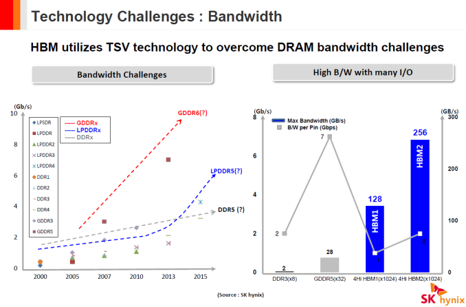
HBM gen 1 memory KGSDs produced by SK Hynix (the only company that makes them commercially) stack four 2 Gb memory dies and operate at 1 Gb/s data rate per pin. AMD uses these KGSDs with 1 GB capacity and 128 GB/s peak bandwidth per stack to build its Fiji GPU system-in-packages (SiPs) and the Radeon R9 Fury/R9 Nano video cards. The graphics adapters have 4 GB of VRAM onboard, not a lot for 2016. While AMD’s flagship video cards do not seem to have capacity issues right now, 4 GB of memory per graphics adapter is a limitation. AMD’s latest graphics cards sport 512 GB/s of memory bandwidth, a massive amount by today’s standards, but even that amount could be a constraint for future high-end GPUs.
HBM Gen 2: Good Thing Gets Better
The second-generation HBM (HBM2) technology, which is outlined by the JESD235A standard, inherits physical 128-bit DDR interface with 2n prefetch architecture, internal organization, 1024-bit input/output, 1.2 V I/O and core voltages as well as all the crucial parts of the original tech. Just like the predecessor, HBM2 supports two, four or eight DRAM devices on a base logic die (2Hi, 4Hi, 8Hi stacks) per KGSD. HBM Gen 2 expands capacity of DRAM devices within a stack to 8 Gb and increases supported data-rates up to 1.6 Gb/s or even to 2 Gb/s per pin. In addition, the new technology brings an important improvement to maximize actual bandwidth.
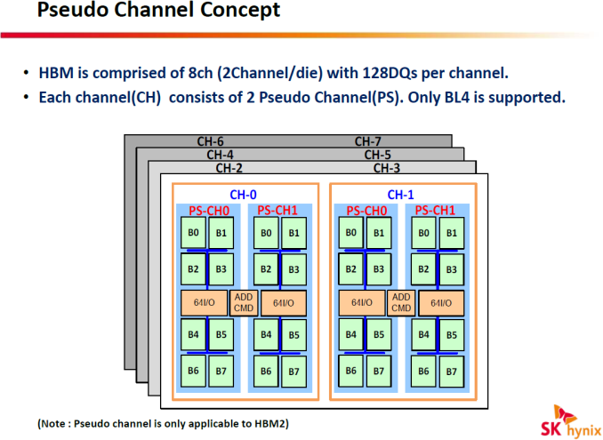
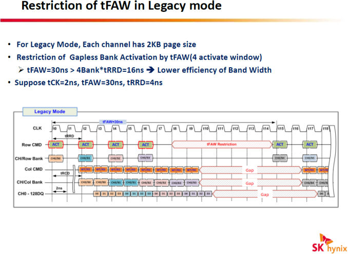
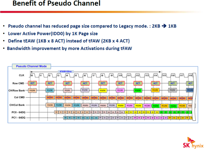
One of the key enhancements of HBM2 is its Pseudo Channel mode, which divides a channel into two individual sub-channels of 64 bit I/O each, providing 128-bit prefetch per memory read and write access for each one. Pseudo channels operate at the same clock-rate, they share row and column command bus as well as CK and CKE inputs. However, they have separated banks, they decode and execute commands individually. SK Hynix says that the Pseudo Channel mode optimizes memory accesses and lowers latency, which results in higher effective bandwidth.
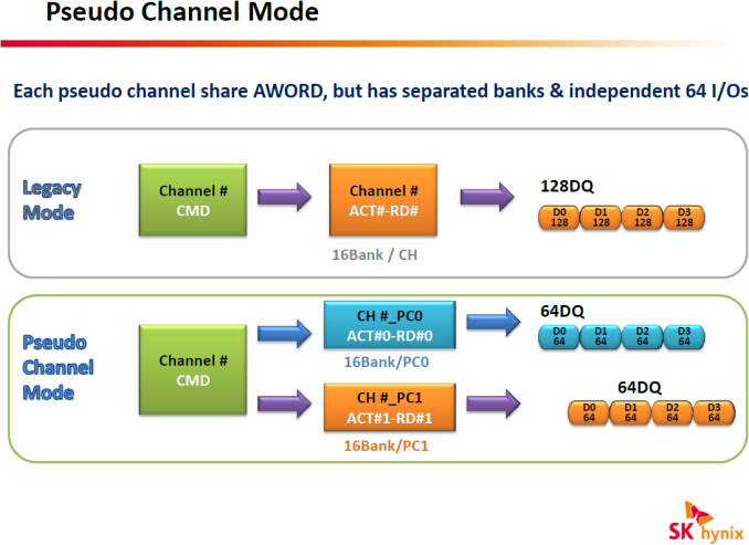
If, for some reason, an ASIC developer believes that Pseudo Channel mode is not optimal for their product, then HBM2 chips can also work in Legacy mode. While memory makers expect HBM2 to deliver higher effective bandwidth than predecessors, it depends on developers of memory controllers how efficient next-generation memory sub-systems will be. In any case, we will need to test actual hardware before we can confirm that HBM2 is better than HBM1 at the same clock-rate.
Additional improvements of HBM2 over the first-gen HBM includes lane remapping modes for hard and soft repair of lanes (HBM1 supports various DRAM cell test and repair techniques to improve yields of stacks, but not lane remapping), anti-overheating protection (KGSD can alert memory controllers of unsafe temperatures) and some other.
The second-generation HBM memory will be produced using newer manufacturing technologies than the first-gen HBM. For example, SK Hynix uses its 29nm process to make DRAM dies for its HBM1 stacks. For HBM2 memory, the company intends to use their 21nm process. Thanks to newer manufacturing technologies and higher effective bandwidth, HBM2 should have higher energy efficiency than HBM1 at its data-rates, but we do not have exact details at this point. In any case, HBM2 is likely to be more energy efficient than GDDR5 and GDDR5X, hence the odds are good that it will be the memory of choice for high-end graphics cards in the future.
Samsung Electronics this week said that it had begun mass production of HBM2 memory, but did not reveal too many details. Samsung's HBM2 KGSD features 4 GB capacity, 2 Gb/s data rate per pin and is based on four 8 Gb DRAM dies. The memory chips will let device manufacturers build SiPs with up to 16 GB of memory. It is noteworthy that Samsung decided to use 8 Gb DRAM dies for its HBM2 stacks. Such decision looks quite logical since with 8 Gb DRAM ICs the company can relatively easily increase or decrease capacity of its KGSDs by altering the number of DRAM layers. The DRAM maker uses its 20nm process to produce its HBM2 DRAM KGSDs. Unfortunately, Samsung did not reveal actual power consumption of the new memory stacks.
| GPU Memory Math | |||||||
| AMD Radeon R9 290X | NVIDIA GeForce GTX Titan X | AMD Radeon R9 Fury X | Samsung's 4-Stack HBM2 based on 8 Gb DRAMs | Theoretical GDDR5X 256-bit sub-system | |||
| Total Capacity | 4 GB | 12 GB | 4 GB | 16 GB | 8 GB | ||
| Bandwidth Per Pin | 5 Gb/s | 7 Gb/s | 1 Gb/s | 2 Gb/s | 10 Gb/s | ||
| Number of Chips/Stacks | 16 | 24 | 4 | 4 | 8 | ||
| Bandwidth Per Chip/Stack | 20 GB/s | 14 GB/s | 128 GB/s | 256 GB/s | 40 GB/s | ||
| Effective Bus Width | 512-bit | 384-bit | 4096-bit | 4096-bit | 256-bit | ||
| Total Bandwidth | 320 GB/s | 336 GB/s | 512 GB/s | 1 TB/s | 320 GB/s | ||
| Estimated DRAM Power Consumption |
30W | 31.5W | 14.6W | n/a | 20W | ||
Larger Package
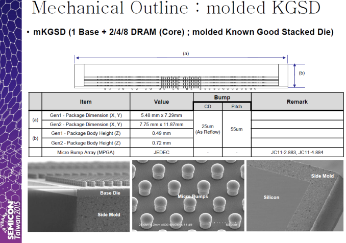
HBM2 memory stacks are not only faster and more capacious than HBM1 KGSDs, but they are also larger. SK Hynix’s HBM1 package has dimensions of 5.48 mm × 7.29 mm (39.94 mm2). The company’s HBM2 chip will have dimensions of 7.75 mm × 11.87 mm (91.99 mm2). Besides, HBM2 stacks will also be higher (0.695 mm/0.72 mm/0.745 mm vs. 0.49 mm) than HBM1 KGSDs, which may require developers of ASICs (e.g., GPUs) to install a heat-spreader on their SiPs to compensate for any differences in height between the memory stacks and GPU die, to protect the DRAM, and to guarantee sufficient cooling for high bandwidth memory.
Larger footprint of the second-gen HBM2 means that the upcoming SiPs with multiple memory stacks will require larger silicon interposers, which means that they are going to be slightly more expensive than SiPs based on the first-gen HBM. Since geometric parameters of staggered microbump pattern of HBM1 and HBM2 are the same, complexity of passive silicon interposers will remain the same for both types of memory. A good news is that to enable 512 GB/s of bandwidth, only two HBM2 stacks are needed, which implies that from bandwidth per mm2 point of view the new memory tech continues to be very efficient.
A slide by FormFactor and Teradyne from their presentation at Semiconductor Wafer Test Workshop 2015
Since SK Hynix’s HBM1 KGSDs are smaller than the company’s HBM2 stacks, they are going to have an advantage over the second-gen high-bandwidth memory for small form-factor SiPs. As a result, the South Korea-based DRAM maker may retain production of its HBM1 chips for some time.
New Use Cases and Industry Support
Thanks to higher capacity and data-rates, HBM2 memory stacks will be pretty flexible when it comes to configurations. For example, it will be possible to build a 2 GB KGSD with 256 GB/s of bandwidth that will use only two 8 Gb memory dies. Such memory stack could be used for graphics adapters designed for notebooks or ultra-small personal computers. Besides, it could be used as an external cache for a hybrid microprocessor with built-in graphics (in the same manner as Intel uses its eDRAM cache to boost performance of its integrated graphics processors). What remains to be seen is the cost of HBM2 stacks that deliver 256 GB/s bandwidth. If HBM2 and the necessary interposer remains as expensive as HBM1, it will likely continue to only be used for premium solutions.
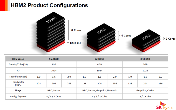
Thanks to a variety of KGSD configurations prepared by DRAM manufacturers, expect new types of devices to start using HBM2. Samsung and SK Hynix believe that in addition to graphics and HPC (high-performance computing) cards, various server, networking and other applications will utilize the new type of memory. As of September, 2015, more than 10 companies were developing system-on-chips (including ASICs, x86 processors, ASSPs and FPGAs) with HBM support, according to SK Hynix.
The first-generation HBM memory delivers great bandwidth and energy efficiency, but it is produced by only one maker of DRAM and is not widely supported by developers of various ASICs. By contrast, Samsung Electronics and SK Hynix, two companies that control well over 50% of the global DRAM output, will make HBM2. Micron Technology yet has to confirm its plans to build HBM2, but since this is an industry-standard type of memory, the door is open if the company wishes to produce it.
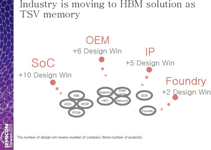
Overall, the industry support for the high bandwidth memory technology is growing. There are 10 companies working on SoCs with HBM support, leading DRAM makers are gearing up to produce HBM2. The potential of the second-gen HBM seems to be rather high, but the costs remain a major concern. Regardless, it will be extremely interesting to see next-generation graphics cards from AMD and NVIDIA featuring HBM2 DRAM and find out what they are capable of because of the new Polaris and Pascal architectures as well as the new type of memory.
Read More ...
Intel Launches Skylake vPro With Intel Authenticate
Intel is launching Intel Authenticate today, and it will require a 6th generation Intel Core processor with vPro. Authenticate will combine several factors of authentication into a single login, which, in theory, should be easier for the end user as well.
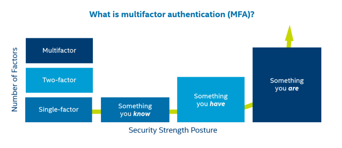
It works by combining “something you know”, which can be a PIN or password, along with “something you have”, which could be a smartphone, and “something you are”, which is biometrics. Once you include many factors, the complexity to lose all of them to the same person goes up quite a bit. The “something you know” can therefore be much easier, such as a PIN, or simple password, since that is not the defining key to the system. IT will be able to choose from multiple factors based on their own policy and preferences. Once configured, the factors are captured, encrypted, matched, and stored in hardware.
The user data never leaves the hardware, reducing the footprint for attack, and removing the chance of accidental misuse by employees. All of the authentication is then done at the hardware level once the user has matched the stored profile. The inclusion of biometrics, especially if they are based on Intel’s RealSense 3D camera systems, also adds in the possibility of having machines auto-lock when the person steps away.
Overall, this is similar to Windows Hello, except with more authentication factors and the resultant matching done on the CPU. There are advantages to this method, but one of the biggest disadvantages is that it will require Skylake class hardware and newer, so you can’t deploy it to older machines. Interestingly it is available on Windows 7, 8.1, and 10, despite Windows 7 and Skylake having a rough start together.
Intel Authenticate is available now for customers to preview.
Source: Intel
Read More ...
AMD Reports Q4 2015 Results And FY 2015 Earnings
| AMD Q3 2015 Financial Results (GAAP) | |||||
| Q4'2015 | Q3'2015 | Q4'2014 | |||
| Revenue | $958M | $1.06B | $1.24B | ||
| Gross Margin | 30% | 23% | 29% | ||
| Operating Income | -$49M | -$158M | -$330M | ||
| Net Income | -$102M | -$197M | -$364M | ||
| Earnings Per Share | -$0.13 | -$0.25 | -$0.47 | ||
On a non-GAAP basis, AMD reports an operating loss for the quarter of $39 million, and a net loss of $79 million. For the full year 2015, the operating loss of $253 million, down from a non-GAAP operating income of $316 million in 2014. This amounts to a per share loss of $0.53 using non-GAAP numbers.
| AMD Q4 2015 Financial Results (Non-GAAP) | |||||
| Q4'2015 | Q3'2015 | Q4'2014 | |||
| Revenue | $958M | $1.06B | $1.24B | ||
| Gross Margin | 30% | 23% | 34% | ||
| Operating Income | -$39M | -$97M | $52M | ||
| Net Income | -$79M | -$136M | $18M | ||
| Earnings Per Share | -$0.10 | -$0.17 | $0.02 | ||
Looking at the individual segments, the Computing and Graphics segment had revenue of $470 million for the quarter, up 11% since last quarter but down 29% year-over-year. AMD had more notebook processor sales compared to last quarter, but lower client processor sales compared to last year. This segment had an operating loss of $99 million, compared to $181 million last quarter and $56 million last year. The inventory write-down last quarter was the main reason for the improvement this quarter, and lower sales caused the year-over-year drop. One good nugget for AMD is that average selling price (ASP) increase sequentially for processors, although it is down year-over-year, but GPU ASP increased both sequentially and year-over-year.
| AMD Q4 2015 Computing and Graphics | |||||
| Q4'2015 | Q3'2015 | Q4'2014 | |||
| Revenue | $470M | $424M | $662M | ||
| Operating Income | -$99M | -$181M | -$56M | ||
The Enterprise, Embedded, and Semi-Custom segment had revenue of $488 million, down 23% from last quarter and 15% year-over-year. Operating income was $59 million, down from $84 million last quarter and $109 million last year. AMD attributes the seasonally lower sales of semi-custom SoCs as the reason for the drop from last quarter, and the year-over-year drop is due to lower game console royalties, and lower server and embedded sales.
| AMD Q4 2015 Enterprise, Embedded and Semi-Custom | |||||
| Q4'2015 | Q3'2015 | Q4'2014 | |||
| Revenue | $488M | $637M | $577M | ||
| Operating Income | $59M | $84M | $109M | ||
The All Other segment had an operating loss of $9 million, an improvement over the $61 million loss last quarter, and a big improvement over the $383 million operating loss in Q4 2014. AMD has made some restructuring charges which affected them last quarter, and the year-over-year improvement was “primarily due to the absence of a goodwill impairment charge, lower restructuring and other special charges, net and a Q4 2014 lower of cost or market inventory adjustment.”
With a less than amazing 2015, for 2016 AMD is resting a lot of hope on their new 4th generation GCN GPU, which they are calling Polaris. On the CPU side, they hope to execute their new Zen platform with a 40% increase in Instructions Per Clock. With AMD getting out of the fab business, they have now been relying on others to move forward on the process side, and we are finally seeing fabs other than Intel now producing FinFET based designs. Clearly AMD has a lot of work to do to not only launch the products, but execute sales of them as well. VR could also be an area where AMD could find some growth, since the requirements for VR will likely drive some GPU sales over the next 12 months.
Read More ...
Available Tags:Microsoft , Wireless , Router , Samsung , Intel , Intel , AMD ,
No comments:
Post a Comment